Diagonal through-flow square cell IGBT and manufacturing method thereof

A flow-through and diagonal technology, applied in the direction of final product manufacturing, sustainable manufacturing/processing, semiconductor/solid-state device manufacturing, etc., can solve problems such as the impact of short-circuit capability of devices

Active Publication Date: 2021-01-01
JIANGSU HAIDONG SEMICON TECH CO LTD
View PDF3 Cites 3 Cited by
  • Summary
  • Abstract
  • Description
  • Claims
  • Application Information

AI Technical Summary

Problems solved by technology

Commonly used chips have different cell types to obtain higher carrier density. At the same time, major mainstream manufacturers have also introduced a square cell structure, which has more conductive channels, but due to the increase of conductive channels, its In the cellular structure, th

Method used


Image

  • Diagonal through-flow square cell IGBT and manufacturing method thereof
  • Diagonal through-flow square cell IGBT and manufacturing method thereof
  • Diagonal through-flow square cell IGBT and manufacturing method thereof

Examples


Embodiment Construction

[0031] In order to make the object, technical solution and advantages of the present invention clearer, the present invention will be described in further detail below in conjunction with the accompanying drawings and embodiments. It should be understood that the specific embodiments described here are only used to explain the present invention, not to limit the present invention.

[0032] IGBT: Insulated Gate Bipolar Transistor

[0033] PECVD: Plasma Enhanced Chemical Vapor Deposition

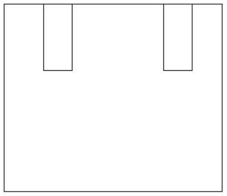
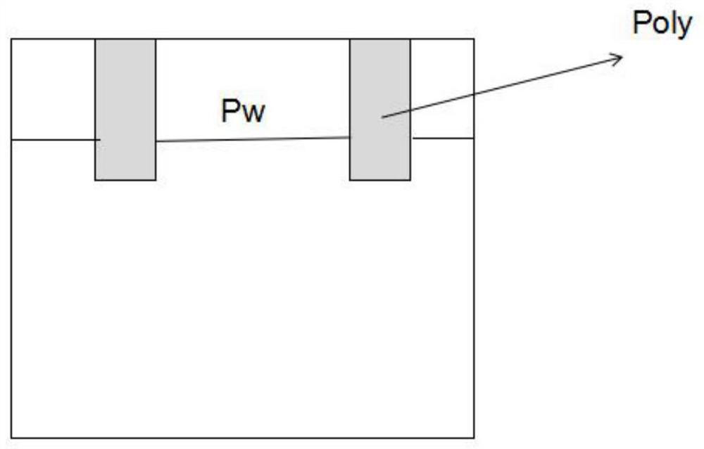
[0034] Trench: groove structure

[0035] Polysilicon: polysilicon

[0036] Boron: boron ion

[0037] Pw area: P-type well area

[0038] Phosphor: phosphorus

[0039] ILD: interlayer dielectric layer

[0040] BPSG: borophosphosilicate glass

[0041] Teos: ethyl orthosilicate

[0042] Emitter: emitter

[0043] FieldStop: field stop layer

[0044] Collector: Collector

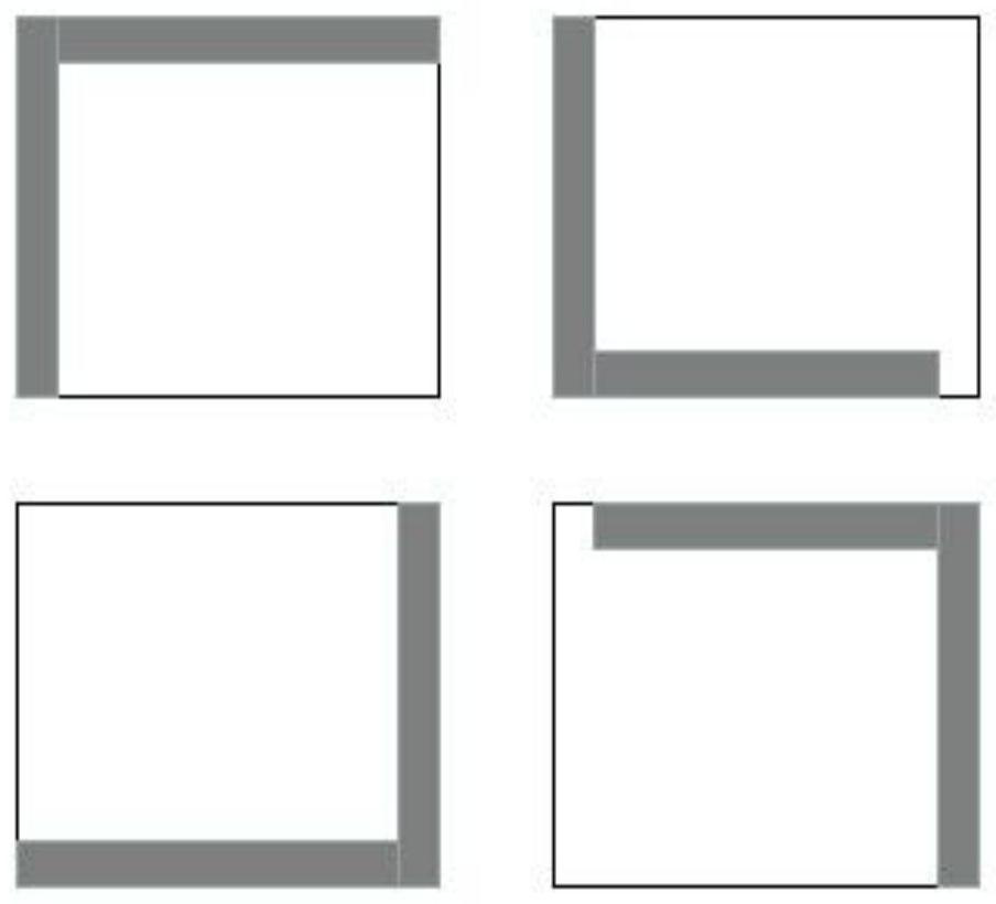
[0045] A method of manufacturing a diagonal flow-through square cell IGBT, comprising the following steps:

[0046] ...


PUM

PropertyMeasurementUnit
Resistivityaaaaaaaaaa
Thicknessaaaaaaaaaa
Thicknessaaaaaaaaaa

Abstract

The invention relates to the technical field of power devices, in particular to a diagonal through-flow square-cell IGBT (Insulated Gate Bipolar Transistor) and a manufacturing method thereof, aims tosolve certain problems existing in the short-circuit capability of devices in the prior art, and is technically characterized by comprising the following steps: S1, selecting a wafer substrate, depositing an initial oxide layer on the surface of the wafer substrate, opening an area needing to be etched, and forming a protection ring region; S2, removing the oxide layer to open the cell region; S3, forming a deep groove structure on the surface of the substrate; S4, forming a gate oxide layer on the surface of the substrate, depositing Polysilicon, and forming a Pw region on the surface of thesubstrate; S5, forming an Nplus region in the deep groove of the substrate; S6, forming an ILD dielectric layer on the surface of the substrate, and etching the dielectric layer to form a contact hole; S7, leading out a metal Emitter electrode; S8, forming a FieldStop layer and a Colletor layer on the back surface of the wafer substrate, and depositing a metal layer to lead out a Colletor electrode. Under the condition that conductive channels are not reduced, the distribution of the conductive channels is controlled, and at most two conductive channels are controlled to be connected, so thatthe generation of current wires is reduced.

Description

technical field [0001] The invention relates to the technical field of power devices, in particular to a diagonal flow-through square cell IGBT and a manufacturing method thereof. Background technique [0002] IGBT (InsulatedGateBipolarTransistor), insulated gate bipolar transistor, is a composite fully-controlled voltage-driven power semiconductor device composed of BJT (bipolar transistor) and MOS (insulated gate field effect transistor), and has high input of MOSFET Impedance and GTR's low conduction voltage drop both advantages. The saturation voltage of GTR is lowered, the carrying current density is large, but the driving current is large; the driving power of MOSFET is small, the switching speed is fast, but the conduction voltage drop is large, and the current carrying density is small. The IGBT combines the advantages of the above two devices, with low driving power and low saturation voltage. It is very suitable for the conversion system with a DC voltage of 600V...

Claims


Application Information

Patent Timeline
IPC IPC(8): H01L21/331H01L29/739
CPCH01L29/66348H01L29/7397Y02P70/50
Inventor 赵家宽黄传伟夏华秋
Owner JIANGSU HAIDONG SEMICON TECH CO LTD
Why Eureka
Try Eureka