Ultraviolet photodiode and preparation method thereof

A technology of ultraviolet light and diodes, applied in circuits, electrical components, semiconductor devices, etc., can solve the problems of low current on/off ratio, weak and low light absorption, small light response rate, etc., and achieve high responsivity rate and high light response rate, high-efficiency photoelectric conversion effect

Active Publication Date: 2021-01-01
WUYI UNIV
View PDF7 Cites 1 Cited by
  • Summary
  • Abstract
  • Description
  • Claims
  • Application Information

AI Technical Summary

Problems solved by technology

However, the current ultraviolet detectors of two-dimensional materials still face small photoresponsivity and low current on / off ratio (on / off ratio reflects the ability of the device to control the current, Defined as the ratio of the device's on-state current to the off-state current) and other issues

Method used


Image

  • Ultraviolet photodiode and preparation method thereof
  • Ultraviolet photodiode and preparation method thereof
  • Ultraviolet photodiode and preparation method thereof

Examples


Embodiment 1

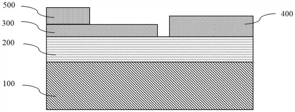
[0042] An ultraviolet photodiode comprising such as figure 1 The structure shown: substrate 100; GaN layer 200, disposed on the upper surface of the substrate 100; Ti 3 C 2 The Schottky contact layer 300 and the ohmic contact layer 400 are relatively arranged on both sides of the upper surface of the GaN layer 200; the metal contact layer 500 is arranged on the Ti 3 C 2 The upper surface of the Schottky contact layer 300 .

[0043] The preparation method of the ultraviolet photodiode is as follows:

[0044] (1) Put the no-clean sapphire substrate into the MOCVD (metal organic chemical vapor deposition) growth chamber, and use trimethylgallium, trimethylaluminum and NH on the sapphire substrate 3 As a source, nitrogen gas is used as a carrier gas, and a GaN nucleation layer of 50 nm, a GaN buffer layer of 200 nm, and an intrinsic GaN layer of 3 μm are epitaxy in sequence to form the GaN layer.

[0045] (2) at Ti 3 C 2 Add ice water to the colloid, centrifuge (3500rpm, 20...

Embodiment 2

[0048] A kind of ultraviolet photodiode, comprises following structure: substrate; GaN layer, is arranged on the upper surface of described substrate; Ti 3 C 2 The Schottky contact layer and the ohmic contact layer are relatively arranged on both sides of the upper surface of the GaN layer; the metal contact layer is arranged on the Ti 3 C 2 top surface of the Schottky contact layer.

[0049] The preparation method of the ultraviolet photodiode is as follows:

[0050] (1) Put the no-clean sapphire substrate into the MOCVD (metal organic chemical vapor deposition) growth chamber, and use trimethylgallium, trimethylaluminum and NH on the sapphire substrate 3 As a source, nitrogen gas is used as a carrier gas, and a GaN nucleation layer of 30 nm, a GaN buffer layer of 150 nm, and an intrinsic GaN layer of 5 μm are epitaxy in sequence to form the GaN layer.

[0051] (2) at Ti 3 C 2 Add ice water to the colloid, centrifuge (3500rpm, 20min), then take out the supernatant; repe...


PUM

PropertyMeasurementUnit
thicknessaaaaaaaaaa
thicknessaaaaaaaaaa
thicknessaaaaaaaaaa

Abstract

The invention belongs to the technical field of semiconductors, and discloses an ultraviolet photodiode and a preparation method thereof. The ultraviolet photodiode comprises the following structures:a substrate; a GaN layer which is arranged on the upper surface of the substrate; a Ti3C2 Schottky contact layer and a ohmic contact layer which are oppositely arranged on the two sides of the uppersurface of the GaN layer; and a metal contact layer which is arranged on the upper surface of the Ti3C2 Schottky contact layer. The ultraviolet photodiode has the advantages of excellent ultraviolet detection performance, high responsivity, high specific detection rate, high response speed and high current switch ratio; and the preparation method does not need a complex metal deposition or sputtering process, does not damage the surface of the semiconductor, and is simple in process.

Description

technical field [0001] The invention belongs to the technical field of semiconductors, in particular to an ultraviolet photodiode and a preparation method thereof. Background technique [0002] Ultraviolet photodetectors (PDs) are fundamental optoelectronic devices capable of converting incident short-wavelength (<400 nm) radiation into electrical signals for photoelectric conversion processing. Based on the capture, recognition and visualization of optical information by detectors, ultraviolet detection technology has a wide range of applications in the fields of military, security communication, imaging, biological detection, chemical analysis and daily life monitoring. Current commercial UV photodiodes are mainly based on vacuum photomultiplier tubes and UV-enhanced silicon photodiodes. However, vacuum devices have disadvantages such as large volume, high operating voltage, and inherent fragility when using vacuum tubes; in addition, the preparation of high-performanc...

Claims


Application Information

Patent Timeline
Patent Type & Authority Applications(China)
IPC IPC(8): H01L31/108H01L31/0224H01L31/18
CPCH01L31/108H01L31/022408H01L31/1852H01L31/1856
Inventor 宋伟东罗幸君李述体陈钊张业龙张弛高研曾庆光何鑫
Owner WUYI UNIV
Why Eureka
Try Eureka