Solution processing series quantum dot light emitting diode based on doped connection layer and manufacturing method of light emitting diode

A quantum dot luminescence and solution processing technology, applied in semiconductor/solid-state device manufacturing, electrical components, circuits, etc., can solve the problems of poor connection layer properties and limited selection, and achieve improved aqueous solution properties, improved wettability, and improved deposition. quality effect

Active Publication Date: 2021-01-08
SOUTHWEST UNIV
View PDF4 Cites 1 Cited by
  • Summary
  • Abstract
  • Description
  • Claims
  • Application Information

AI Technical Summary

Problems solved by technology

[0006] One of the objectives of the present invention is to provide a solution-processed series quantum dot light-emitting diode based on a doped connection layer, which solves the problems of limited material selection for the connection layer and poor properties of the connection layer in the existing solution-processed quantum dot light-emitting diodes. A simple and effective method to improve the performance of solution-processed quantum dot light-emitting diodes is proposed

Method used


Image

  • Solution processing series quantum dot light emitting diode based on doped connection layer and manufacturing method of light emitting diode
  • Solution processing series quantum dot light emitting diode based on doped connection layer and manufacturing method of light emitting diode
  • Solution processing series quantum dot light emitting diode based on doped connection layer and manufacturing method of light emitting diode

Examples


Embodiment

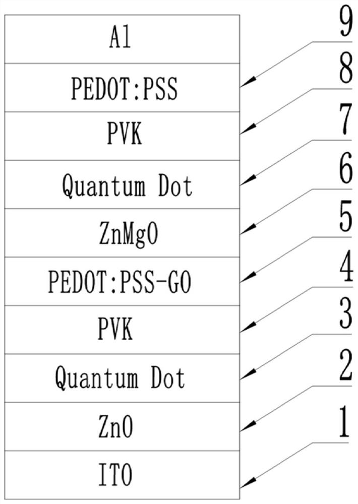
[0046] A solution-processed tandem quantum dot light-emitting diode based on a doped connection layer, basically as attached figure 1 Shown: Includes bottom device and top device. The bottom device includes a cathode 1 , a first electron injection layer 2 , a first quantum dot light-emitting layer 3 , a first hole transport layer 4 and a first hole injection layer 5 which are stacked sequentially from bottom to top. The top device includes a second electron injection layer 6 , a second quantum dot light-emitting layer 7 , a second hole transport layer 8 , a second hole injection layer 9 and an anode which are stacked sequentially from bottom to top. The first hole injection layer 5 of the bottom device and the second electron injection layer 6 of the top device are laminated, and the first hole injection layer 5 and the second electron injection layer 6 are used as the solution processing doping connection layer of the quantum dot light-emitting diode in series .

[0047] In...


PUM

PropertyMeasurementUnit
sizeaaaaaaaaaa
current efficiencyaaaaaaaaaa
surface roughnessaaaaaaaaaa

Abstract

The invention belongs to the technical field of quantum dot light-emitting diodes, and particularly relates to a solution processing series quantum dot light-emitting diode based on a doped connectionlayer and a manufacturing method of the solution processing series quantum dot light-emitting diode. The light emitting diode comprises a bottom device and a top end device; the bottom device comprises a cathode, a first electron injection layer, a first quantum dot light-emitting layer, a first hole transport layer and a first hole injection layer which are sequentially stacked from bottom to top. The top end device comprises a second electron injection layer, a second quantum dot light-emitting layer, a second hole transport layer, a second hole injection layer and an anode which are sequentially stacked from bottom to top, the first hole injection layer of the bottom device and the second electron injection layer of the top end device are stacked, the first hole injection layer is madeof a PEDOT: PSS-GO solution. and the second electron injection layer is made of a solution containing ZnMgO. The invention provides an effective method for improving the performance of a solution processing quantum dot light emitting diode.

Description

technical field [0001] The invention belongs to the technical field of quantum dot light-emitting diodes, and in particular relates to a solution-processed serial quantum-dot light-emitting diode based on a doped connection layer and a manufacturing method thereof. Background technique [0002] Quantum dots are one of the new materials—solution nanocrystals. Solution nanocrystals have the dual properties of crystal and solution. Unlike other nanocrystalline materials, quantum dots are based on semiconductor crystals. The size is between 1 and 100 nanometers, and each particle is a single crystal. The name of quantum dots comes from the quantum confinement effect or quantum size effect of semiconductor nanocrystals. When semiconductor crystals are as small as nanometers, different sizes can emit light of different colors. For example, semiconductor nanocrystals such as cadmium selenide emit blue light at 2 nanometers, red light at 8 nanometers, and green, yellow, orange, e...

Claims


Application Information

Patent Timeline
Patent Type & Authority Applications(China)
IPC IPC(8): H01L51/50H01L51/54H01L51/56
CPCH10K85/1135H10K50/115H10K50/17H10K50/171H10K71/00
Inventor 雷衍连陈历相
Owner SOUTHWEST UNIV
Why Eureka
Try Eureka