Heterogeneously integrated system-in-package structure and packaging method
A system-level packaging and packaging method technology, which is applied in the direction of semiconductor/solid-state device components, semiconductor devices, electrical components, etc., can solve the problem that the flatness of the tube and shell processing of the double-cavity structure is difficult to control, and the miniaturization and light weight cannot be achieved. Requirements, unfavorable production cost control and mass production, to achieve the effect of reducing development cost and cycle, reducing flatness risk, and solving packaging process problems
- Summary
- Abstract
- Description
- Claims
- Application Information
AI Technical Summary
Problems solved by technology
Method used
Image
Examples
Embodiment 1
[0058] This example provides a heterogeneous integrated system-in-package structure, which includes two cavities.
[0059] Specifically, such as figure 1 As shown, the first cavity 4 is formed by digging a cavity on one side of the ceramic substrate 1 ; the second cavity 3 is formed by welding the Kovar ring 2 on the other side of the ceramic substrate 1 .
[0060] At the opening of the first cavity 4 , a first cover plate 41 for closing the first cavity 4 is assembled.
[0061] At the opening of the second cavity 3 , a second cover plate 31 for closing the second cavity 3 is assembled.
[0062] At least one chip 5 is respectively arranged in the first cavity 4 and the second cavity 3 , and the chip 5 is bonded to the surface of the ceramic substrate 1 through the conductive glue 7 .
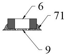
[0063] At least one passive discrete component 6 is disposed in the first cavity 4 or the second cavity 3 , and the passive discrete component 6 is bonded to the surface of the ceramic substra...
Embodiment 2
[0089] This example provides a packaging method for a heterogeneously integrated system-in-package structure, which at least includes the following steps, and the flow of the steps is as follows: Figure 10 Shown:
[0090] Step 1) Shell Handling
[0091] A ceramic substrate 1 is provided, and a cavity is dug on one side to form a first cavity 4; a Kovar ring 2 is provided on the other side of the ceramic substrate 1 to form a second cavity 3, such as Figure 1~2 shown;
[0092] Among them, such as Figure 5~8 As shown, when the first cavity 4 is formed, a first reinforcing rib 42 integrally formed with the ceramic base 1 is formed at the same time, which is used to divide the first cavity 4 into two chambers; when the second cavity 3 is formed At the same time, a second rib 32 is welded on the surface of the ceramic base 1 of the second cavity 3, which is used to divide the second cavity 3 into two chambers; the first rib 42 and the second rib 32 are vertically arranged . ...
PUM
| Property | Measurement | Unit |
|---|---|---|
| thickness | aaaaa | aaaaa |
| thickness | aaaaa | aaaaa |
Abstract
Description
Claims
Application Information
 - R&D
- Intellectual Property
- Life Sciences
- Materials
- Tech Scout
- Unparalleled Data Quality
- Higher Quality Content
- 60% Fewer Hallucinations
Browse by: Latest US Patents, China's latest patents, Technical Efficacy Thesaurus, Application Domain, Technology Topic, Popular Technical Reports.
© 2025 PatSnap. All rights reserved.Legal|Privacy policy|Modern Slavery Act Transparency Statement|Sitemap|About US| Contact US: help@patsnap.com


