Composite substrate, composite film and preparation method thereof

A composite substrate and composite film technology, applied in electrical components, impedance networks, etc., can solve problems such as the influence of substrate materials and the insufficient trap density.

Active Publication Date: 2021-01-22
JINAN JINGZHENG ELECTRONICS
View PDF5 Cites 2 Cited by
  • Summary
  • Abstract
  • Description
  • Claims
  • Application Information

AI Technical Summary

Problems solved by technology

However, the introduction of the trap layer has caused new problems. Specifically, on the one hand, the trap density may not be sufficient due to the influence of the film layer preparation process in actual manufacturing; on the other hand, there are also requirements for other properties of the substrate in some device applications. , such as the sound velocity in the surface acoustic wave filter, the refractive index in the optical device, etc., the introduction of the trap film layer may have some adverse effects on these properties of the substrate material

Method used


Image

  • Composite substrate, composite film and preparation method thereof
  • Composite substrate, composite film and preparation method thereof
  • Composite substrate, composite film and preparation method thereof

Examples


Embodiment 1

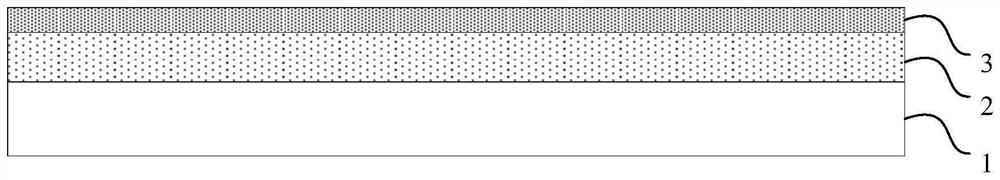
[0167] Using high-resistance silicon substrate (resistivity>2500Ω·cm) as the semiconductor substrate, using the RCA method to clean the process surface to obtain a clean surface;

[0168] Deposit a polysilicon layer as a trap layer on the process surface of the processed high-resistance silicon substrate by LPCVD process, the deposition temperature is 580°C-590°C, and the deposition thickness is 300nm;

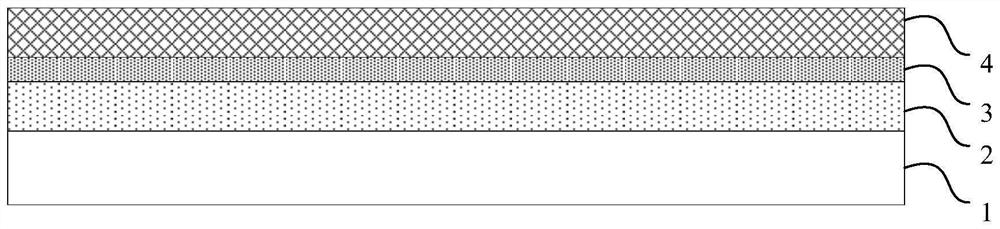
[0169] Implant C into the polysilicon layer + Form a trap enhancement layer, adjust the implantation depth to about 100nm, the implanted ions will expand in the depth direction, and present a Gaussian distribution near the implantation depth, based on the total molar weight of the trap enhancement layer, wherein the dopant atoms The molar percentage is 5%;

[0170] The product obtained in the above steps is annealed at 700 ° C ~ 950 ° C, and the annealing atmosphere is N 2 , the annealing time is 4h, and the C element will be more uniformly distributed in the polysilicon fil...

Embodiment 2

[0176] Using silicon carbide substrate (resistivity>2500Ω·cm) as the semiconductor substrate, the process surface is cleaned by RCA method to obtain a clean surface;

[0177] Deposit a polysilicon layer as a trap layer on the process surface of the processed high-resistance silicon substrate by LPCVD process, the deposition temperature is 640°C-650°C, and the deposition thickness is 3000nm;

[0178] Implant C into the polysilicon layer + Form a trap enhancement layer, adjust the implantation depth to about 500nm, the implanted ions will expand in the depth direction, and present a Gaussian distribution near the implantation depth, based on the total molar weight of the trap enhancement layer, wherein the dopant atoms The molar percentage is 30%;

[0179] The product obtained in the above steps is annealed at 700 ° C ~ 950 ° C, and the annealing atmosphere is N 2 , the annealing time is 4h, and the C element will be more uniformly distributed in the polysilicon film layer due...

Embodiment 3

[0185] GaAs substrate (resistivity>2500Ω·cm) is used as the semiconductor substrate, and the process surface is cleaned by RCA method to obtain a clean surface;

[0186]Deposit a polycrystalline Ge layer as a trap layer on the process surface of the processed high-resistance silicon substrate by PECVD process, the deposition temperature is 200°C-500°C, and the deposition thickness is 1000nm;

[0187] Implanting Ar into the polycrystalline Ge layer + Form a trap enhancement layer, and adjust the implantation depth to about 100nm to 500nm. The implanted ions will expand in the depth direction and present a Gaussian distribution near the implantation depth. Based on the total molar weight of the trap enhancement layer, the doped The molar percentage of atoms is 0.5%;

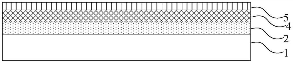
[0188] Deposition of SiO on trap enhancement layer by PECVD method 2 film layer as insulating layer, SiO 2 The thickness of the film layer is 5 μm;

[0189] to SiO 2 The film layer is subjected to CMP treatmen...


PUM

PropertyMeasurementUnit
thicknessaaaaaaaaaa
thicknessaaaaaaaaaa
thicknessaaaaaaaaaa

Abstract

The invention provides a composite substrate, a composite film and a preparation method and application of the composite substrate and the composite film. A trap enhancement layer is additionally arranged on one side of a trap layer near an interface of a trap layer insulating layer or an interface of a trap layer active layer; a trap enhancement layer insulating layer or a trap enhancement layeractive layer structure is formed, and doping atoms are doped in the trap enhancement layer, so compared with the trap layer, the trap enhancement layer has the advantages that the defect density is increased, the PSC inhibition effect is improved, the electric loss is reduced, and the sound velocity is improved; therefore, the sound velocity difference with the insulating layer / active layer is increased, the reflection effect of sound waves at the interface of the insulating layer trap enhancement layer or the interface of the active layer trap enhancement layer is enhanced, the sound wave leakage is reduced, the performance of the device is improved, and two performance improvement effects are realized through one-step process treatment.

Description

technical field [0001] The application belongs to the field of semiconductor devices, in particular to a composite substrate, a composite film and a preparation method thereof. Background technique [0002] Thin-film materials can meet the requirements of electronic components in the direction of miniaturization, low power consumption, and high performance. Therefore, they have become more and more important materials in today's semiconductor industry. In recent years, a thin-film structure material called on insulator has attracted more and more attention from the industry. This material mainly includes an active layer, an insulating layer and a substrate layer in turn. layer to realize the transmission of light, electricity, sound and other signals. This thin-film structure material on an insulator exhibits good application performance in CPU chips, memories, amplifiers, filters, modulators and other devices. [0003] When the insulating material is in direct contact wit...

Claims


Application Information

Patent Timeline
Patent Type & Authority Applications(China)
IPC IPC(8): H03H9/25H03H9/02H03H3/08
CPCH03H9/02574H03H9/02614H03H9/02818H03H9/25H03H3/08
Inventor 李真宇杨超李洋洋韩智勇张涛张秀全
Owner JINAN JINGZHENG ELECTRONICS
Why Eureka
Try Eureka