
One-step synthesis of one-dimensional indium oxide/indium sulfide composite semiconductor nanofibers

A compound semiconductor and nanofiber technology, applied in the direction of carbon monoxide, chemical instruments and methods, chemical/physical processes, etc., to achieve the effects of large electrostatic repulsion, simple and time-saving methods, and high product selectivity

Active Publication Date: 2021-08-31
FUZHOU UNIV
View PDF6 Cites 0 Cited by
  • Summary
  • Abstract
  • Description
  • Claims
  • Application Information

AI Technical Summary

Problems solved by technology

For the electrospinning one-step method, the sulfur source is directly added to the spinning solution and calcined to obtain In 2 S 3 / In 2 o 3 The method of heterojunction photocatalyst has not been reported

Method used


Image

  • One-step synthesis of one-dimensional indium oxide/indium sulfide composite semiconductor nanofibers
  • One-step synthesis of one-dimensional indium oxide/indium sulfide composite semiconductor nanofibers
  • One-step synthesis of one-dimensional indium oxide/indium sulfide composite semiconductor nanofibers

Examples


Embodiment 1

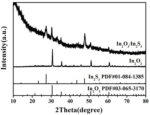
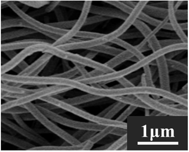
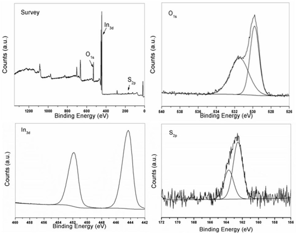
[0024] 0.5 g of indium trichloride tetrahydrate (InCl 3 4H 2 O) and 0.2 g of thioacetamide were sequentially added to a mixed solution of 10 mL of absolute ethanol, ethylene glycol and N,N-dimethylformamide (volume ratio 2:1:2), and stirred evenly; 1 g polyvinylpyrrolidone was added to the above solution to obtain a homogeneous precursor spinning solution, which was jet-spun in an electrospinning device with a spinneret aperture of 0.5 mm; the receiving distance was 15 cm, and the voltage was 10 kV. The speed was 0.1 mm / min; the prepared precursor fibers were placed in a tube furnace and calcined at 400 °C for 2 h under an Ar atmosphere with a heating rate of 2 °C / min to obtain one-dimensional In 2 o 3 / In 2 S 3 Composite semiconducting nanofibers with a diameter of 250-300 nm.

Embodiment 2

[0026] 0.5 g of indium trichloride tetrahydrate (InCl 3 4H 2 O) and 0.4 g of thioacetamide were sequentially added to a mixed solution of 10 mL of absolute ethanol, ethylene glycol and N,N-dimethylformamide (volume ratio 2:1:2), and stirred evenly; 0.9 g of polyvinylpyrrolidone was added to the above solution to obtain a homogeneous precursor spinning solution, which was jet-spun in an electrospinning device with a spinneret aperture of 0.5 mm; the receiving distance was 15 cm, and the voltage was 15 kV. The speed was 0.15 mm / min; the prepared precursor fibers were placed in a tube furnace and calcined at 500 °C for 2 h under an Ar atmosphere with a heating rate of 2 °C / min to obtain one-dimensional In 2 o 3 / In 2 S 3 Composite semiconducting nanofibers with a diameter of 200-250 nm.

Embodiment 3

[0028] 0.5 g of indium trichloride tetrahydrate (InCl 3 4H 2 O) and 0.6 g of thioacetamide were sequentially added to a mixed solution of 10 mL of absolute ethanol, ethylene glycol and N,N-dimethylformamide (volume ratio 2:1:2), and stirred evenly; 1.1 g of polyvinylpyrrolidone was added to the above solution to obtain a homogeneous precursor spinning solution, which was jet-spun in an electrospinning equipment with a spinneret aperture of 0.5 mm; the receiving distance was 15 cm, and the voltage was 13 kV. The speed was 0.2 mm / min; the prepared precursor fibers were placed in a tube furnace and calcined at 600 °C for 2 h under an Ar atmosphere with a heating rate of 2 °C / min to obtain one-dimensional In 2 o 3 / In 2 S 3 Composite semiconducting nanofibers with a diameter of 270-320 nm.


PUM

PropertyMeasurementUnit
diameteraaaaaaaaaa
diameteraaaaaaaaaa
diameteraaaaaaaaaa

Abstract

The present invention provides one-dimensional In 2 o 3 / In 2 S 3 One-step synthesis method of composite semiconductor nanofibers, by designing the precursor spinning solution reaction system, jet spinning in electrospinning equipment; the prepared precursor fibers are calcined at high temperature in a tube furnace to obtain one-dimensional In 2 o 3 / In 2 S 3 Composite semiconducting nanofibers. The present invention obtains one-dimensional In 2 o 3 / In 2 S 3 Composite semiconducting nanofibers. The preparation process of the present invention is simple, easy to control, wide sources of selected raw materials, low in price, meets actual production needs, and has great application potential in the fields of gas sensing, photocatalysis, electrocatalysis, new semiconductor materials and the like.

Description

technical field [0001] The invention belongs to the technical field of material chemistry and photocatalyst, in particular to a one-dimensional In 2 o 3 / In 2 S 3 One-step synthesis of composite semiconducting nanofibers. Background technique [0002] With the rapid development of industry and the gradual increase of fossil energy consumption, CO 2 Emissions are increasing day by day, which in turn causes a series of phenomena such as the greenhouse effect, global warming, glacier melting and sea level rise, which have caused serious harm to the earth's environment. Therefore, how to effectively collect and utilize CO 2 , has become one of the important strategic issues of global economic development. [0003] Photocatalytic technology is CO 2 The innovative technology of conversion and utilization can use solar energy to excite semiconductor photocatalytic materials to generate photogenerated electrons-holes, and convert greenhouse gas CO 2 Revert to hydrocarbon fue...

Claims


Application Information

Patent Timeline
Patent Type & Authority Patents(China)
IPC IPC(8): B01J27/04B01J35/02B01J35/06B01J37/08B01J37/34C01B32/40B01J35/00
CPCB01J27/04B01J37/342B01J37/082C01B32/40B01J35/58B01J35/40B01J35/39
Inventor 何运慧连希凡刘明华肖光参陈志鑫
Owner FUZHOU UNIV
Learn More