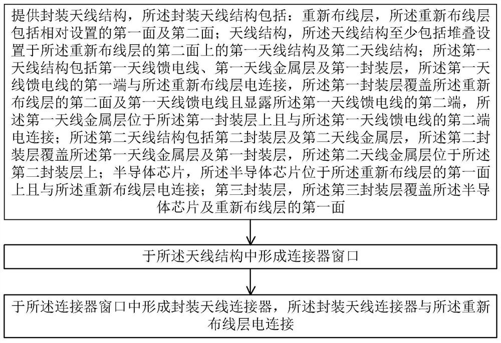
Packaged antenna module and preparation method thereof
An antenna module and antenna technology, applied in antennas, antenna components, antenna supports/mounting devices, etc., can solve the problems of packaged antenna signal loss, location layout limitations, etc., to reduce signal loss and improve the overall competitive advantage , the effect of improving flexibility
- Summary
- Abstract
- Description
- Claims
- Application Information
AI Technical Summary
Problems solved by technology
Method used
Image

Examples
Embodiment 1
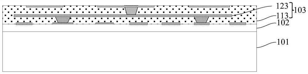
[0068] Such as Figure 8 , this embodiment provides an antenna-in-package module, the antenna-in-package module includes a rewiring layer 103 , an antenna structure, a semiconductor chip 107 , a third packaging layer 108 and an antenna-in-package connector 111 . Wherein, the rewiring layer 103 includes a first surface and a second surface opposite to each other; the antenna structure includes a connector window 109 and at least a first antenna structure stacked on the second surface of the rewiring layer 103 104 and a second antenna structure 106, the first antenna structure 104 includes a first antenna feeder 1141, a first antenna metal layer 1341 and a first encapsulation layer 124, the first end of the first antenna feeder 1141 is connected to the The rewiring layer 103 is electrically connected, the first encapsulation layer 124 covers the first antenna feeder 1141 and exposes the second end of the first antenna feeder 1141, and the first antenna metal layer 1341 is locate...
Embodiment 2
[0110] Such as Figure 11 , this embodiment provides a schematic structural diagram of a packaged antenna module, the main difference from Embodiment 1 is that the position of the connector window in the packaged antenna module is different, so as to enlarge the packaged antenna connector selection range.
[0111] Wherein, the antenna-in-package module includes a rewiring layer 203 , an antenna structure, a semiconductor chip 207 , a third packaging layer 208 and an antenna-in-package connector 211 . Wherein, the rewiring layer 203 includes a first surface and a second surface opposite to each other; the antenna structure includes a connector window 209 and at least a first antenna structure stacked on the second surface of the rewiring layer 203 204 and a second antenna structure 206, the first antenna structure 204 includes a first antenna feeder 214, a first antenna metal layer 234 and a first encapsulation layer 224, the first end of the first antenna feeder 214 is connec...
PUM
 Abstract
Description
Claims
Application Information
 - Generate Ideas
- Intellectual Property
- Life Sciences
- Materials
- Tech Scout
- Unparalleled Data Quality
- Higher Quality Content
- 60% Fewer Hallucinations
Browse by: Latest US Patents, China's latest patents, Technical Efficacy Thesaurus, Application Domain, Technology Topic, Popular Technical Reports.
© 2025 PatSnap. All rights reserved.Legal|Privacy policy|Modern Slavery Act Transparency Statement|Sitemap|About US| Contact US: help@patsnap.com