Double-ended photoelectric memory and preparation method and application thereof

A memory and optoelectronic technology, used in semiconductor/solid-state device manufacturing, circuits, electrical components, etc., can solve problems such as the decrease of floating gate-to-gate coupling ratio and inter-unit interference, achieve strong light absorption capability, improve integration density, and promote development. Effect

Active Publication Date: 2021-01-29
TIANJIN UNIVERSITY OF TECHNOLOGY
View PDF6 Cites 2 Cited by
  • Summary
  • Abstract
  • Description
  • Claims
  • Application Information

AI Technical Summary

Problems solved by technology

Due to the continuous shrinking of device size, especially the sharp drop of gate coupling ratio (GCR) of floating gate (heavily doped

Method used


Image

  • Double-ended photoelectric memory and preparation method and application thereof
  • Double-ended photoelectric memory and preparation method and application thereof
  • Double-ended photoelectric memory and preparation method and application thereof

Examples


Embodiment 1

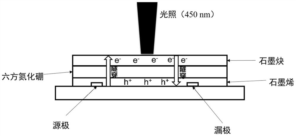
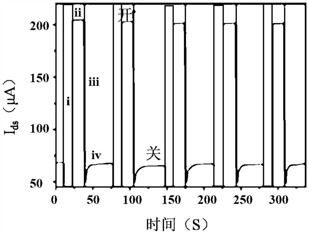
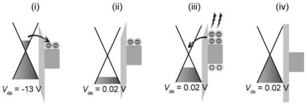
[0044] see figure 1 , this embodiment provides a double-terminal photoelectric memory, including an insulating substrate, a conductive channel, a barrier layer, a tunneling layer and a top photosensitive floating gate sequentially arranged from bottom to top, the insulating substrate and the conductive channel An opposing source electrode (source) and a drain electrode (drain) are provided therebetween.

[0045] Wherein, the insulating substrate is a silicon wafer, the conductive channel is graphene (Gr), the barrier layer and the tunneling layer are hexagonal boron nitride (hBN), and the top photosensitive floating gate is graphdiyne ( GDY), the source electrode and the drain electrode are both Cr / Au composite layers.

[0046] The preparation method of the double-terminal photoelectric memory comprises the following steps:

[0047](1) Graphene and hexagonal boron nitride were grown by chemical vapor deposition with thicknesses of 0.5 nm and 5 nm, respectively.

[0048] (2)...

Embodiment 2

[0059] see Figure 7 , this embodiment provides a flexible double-terminal photoelectric memory, including a flexible insulating substrate, a conductive channel, a barrier layer, a tunneling layer and a top photosensitive floating gate sequentially arranged from bottom to top, the insulating substrate and the conductive channel Opposing source and drain electrodes are disposed between the tracks.

[0060] Wherein, the flexible insulating substrate is PET, the conductive channel is graphene (Gr), the barrier layer and the tunneling layer are hexagonal boron nitride (hBN), and the top photosensitive floating gate is graphite Alkyne (GDY), the source and drain electrodes are both TIO films.

[0061] The preparation method of the flexible double-terminal photoelectric memory comprises the following steps:

[0062] (1) Graphene and hexagonal boron nitride with thicknesses of 0.5 nm and 5 nm were grown by chemical vapor deposition, respectively.

[0063] (2) The opposite source a...


PUM

PropertyMeasurementUnit
Thicknessaaaaaaaaaa
Thicknessaaaaaaaaaa
Thicknessaaaaaaaaaa

Abstract

The invention discloses a double-ended photoelectric memory and a preparation method and application thereof, the double-ended photoelectric memory comprises a conductive channel, a barrier layer, a tunneling layer and a top photosensitive floating gate which are sequentially arranged from bottom to top, and the top photosensitive floating gate is graphdiyne. According to the memory, graphdiyne serves as a top photosensitive floating gate, the graphdiyne has a natural band gap, strong light absorption capacity and a high-density state, a large number of electron hole pairs are generated underillumination, more charges can be stored, gate coupling ratio degradation and inter-unit interference are inhibited, so that the data storage capacity of the memory is improved and the working voltageis reduced. Meanwhile, the memory can be made into flexible equipment to be used for a wearable system, so that the miniaturization of the equipment is facilitated, and the integration density is improved.

Description

technical field [0001] The invention belongs to the technical field of two-dimensional floating gate memories, and in particular relates to a double-terminal photoelectric memory and a preparation method and application thereof. Background technique [0002] With the advent of the 5G era, information storage has attracted more and more attention. In the digital world, humans generate huge amounts of data every year. In order to process such a large amount of data, it is crucial to develop high-performance, low-power, and low-cost memories to meet the needs of people's future lives. [0003] Memory can be classified according to many functional criteria, and can be divided into volatile memory and non-volatile memory according to the ability to retain data after power disconnection. In volatile memory, the information eventually disappears when the power is turned off, so the device that stores the data is required to be periodically refreshed. Its main types are static ra...

Claims


Application Information

Patent Timeline
IPC IPC(8): H01L29/788H01L21/336
CPCH01L29/788H01L29/66825
Inventor 鲁统部于美溪陈旭东
Owner TIANJIN UNIVERSITY OF TECHNOLOGY
Why Eureka
Try Eureka