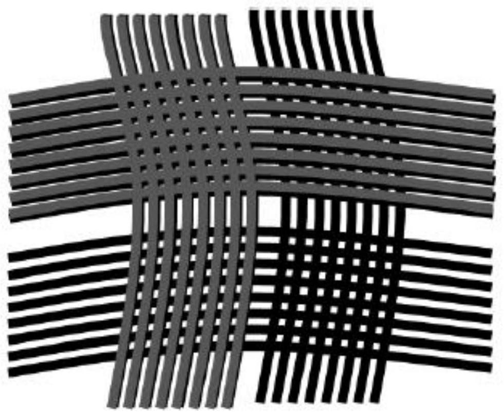
Optical anti-counterfeiting mark and preparation method thereof
An optical anti-counterfeiting and marking technology, which is applied in the field of dyeing anti-counterfeiting, can solve the problems of easy loss of anti-counterfeiting function, printing anti-counterfeiting production technology is easy to be copied, and it is difficult to make anti-counterfeiting marks, so as to achieve environmental protection and healthy color rendering effect and high color saturation , Strong anti-friction ability
- Summary
- Abstract
- Description
- Claims
- Application Information
AI Technical Summary
Problems solved by technology
Method used
Image
Examples
preparation example Construction
[0050] The invention provides a method for preparing an optical anti-counterfeit mark, comprising the following steps:
[0051] Step 1, use white silk as the substrate, cover a hollow mask on the substrate surface, the hollow mask has the pattern of the anti-counterfeiting mark prepared according to the needs, and then use the electron beam evaporation method to evaporate titanium films of different thicknesses in different regions , and according to the needs of different colors, different regions are masked at different thicknesses, so as to obtain samples with titanium thin films.
[0052] Step 2, vapor-deposit silicon thin films of different thicknesses on the sample, and cover different areas at different thicknesses according to the needs of different colors, so as to obtain an optical anti-counterfeiting mark with a Ti-Si multilayer film structure evaporated, and then Samples with optical anti-counterfeiting marks were obtained.
[0053] In the present invention, the t...
Embodiment 1
[0060] The optical mask of the Chinese face pattern that adopts in the present embodiment can be by oneself hand-cut or customize to relevant commercial company.
[0061] Figure 8 In Example 1 of the present invention, a 100nm Ti film was evaporated on white silk, and 40nm, 100nm, and 132nm (corresponding to the left face) and (40nm, 120nm, 144nm, corresponding to the right face) were respectively evaporated on ①, ②, and ③. silicon thin film.
[0062] Step 1, using white silk as a substrate, covering a hollow mask on the surface of the substrate, the hollow mask has a pattern of anti-counterfeiting marks prepared according to needs, and then adopts an electron beam evaporation method to evaporate a 100nm titanium film to obtain a Samples of titanium thin films.
[0063] Step 2: Evaporate silicon films of 40nm, 100nm, and 132nm (corresponding to the left face) (40nm, 120nm, 144nm, corresponding to the right face) on the sample, such as Figure 8 As shown, and according to t...
Embodiment 2
[0066] The optical mask with the Fudan University emblem pattern used in this embodiment can be cut by hand or customized from a relevant commercial company.
[0067] Step 1, use black silk as the substrate, put the substrate into the electron beam evaporation equipment for evaporation, first use the electron beam evaporation method to evaporate a layer of 5nm titanium film, and then evaporate a layer of 20nm on the titanium film silicon thin film, thus obtaining a sample with two thin films.
[0068] Step 2, covering the surface of the sample with an optical mask with the Fudan University emblem pattern.
[0069] Step 3: Evaporate 144nm, 180nm, 215nm, 270nm, 320nm SiO on ①②③④⑤ respectively 2 thin film, thus obtained evaporated with Ti-Si-SiO 2 The optical anti-counterfeiting mark of the multi-layer film structure, and then obtain the sample with the optical anti-counterfeiting mark.
[0070] Figure 9 In Example 2 of the present invention, a 5nm Ti film is deposited on bl...
PUM
| Property | Measurement | Unit |
|---|---|---|
| thickness | aaaaa | aaaaa |
| thickness | aaaaa | aaaaa |
| thickness | aaaaa | aaaaa |
Abstract
Description
Claims
Application Information
 - R&D
- Intellectual Property
- Life Sciences
- Materials
- Tech Scout
- Unparalleled Data Quality
- Higher Quality Content
- 60% Fewer Hallucinations
Browse by: Latest US Patents, China's latest patents, Technical Efficacy Thesaurus, Application Domain, Technology Topic, Popular Technical Reports.
© 2025 PatSnap. All rights reserved.Legal|Privacy policy|Modern Slavery Act Transparency Statement|Sitemap|About US| Contact US: help@patsnap.com


