Method for measuring PDE and Pct spatial two-dimensional distribution of silicon photomultiplier

A technology of silicon photomultiplier tube and measurement method, which is applied in the field of weak light detection and can solve problems such as expensive

Pending Publication Date: 2021-03-02
XI'AN POLYTECHNIC UNIVERSITY
View PDF11 Cites 6 Cited by
  • Summary
  • Abstract
  • Description
  • Claims
  • Application Information

AI Technical Summary

Problems solved by technology

Jelena Ninkovic et al. reported that by using a high-resolution infrared CCD camera for infrared photon emission imaging to directly capture a two-dimensional map of the near-infrared photon emission intensity of the SiPM high-field region, however, this infrared CCD is very expensive and requires low temperature Refrigeration in response to infrared photons

Method used


Image

  • Method for measuring PDE and Pct spatial two-dimensional distribution of silicon photomultiplier
  • Method for measuring PDE and Pct spatial two-dimensional distribution of silicon photomultiplier
  • Method for measuring PDE and Pct spatial two-dimensional distribution of silicon photomultiplier

Examples


Embodiment

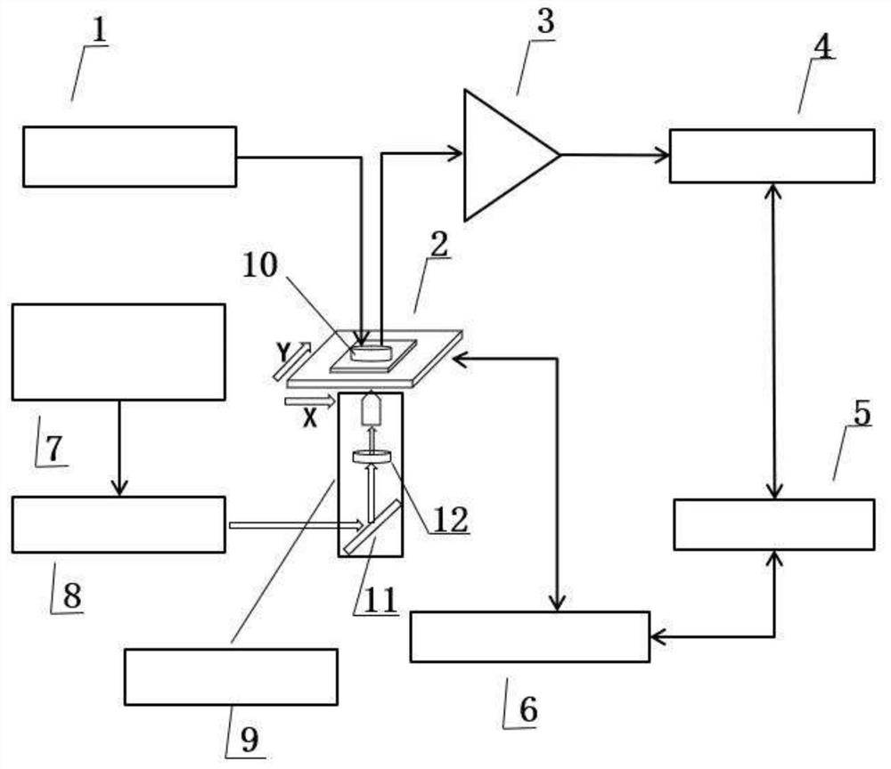
[0059] As shown in Figure 1, the types of silicon photomultiplier tubes 10 used in this embodiment are S12571-100C, S12571-025C and S12571-010C, and the unit sizes are 100×100um 2 ,25×25um 2 and 10×10um 2 ; Hamamatsu Photonics K.K., (made in Japan); piezoelectric ceramic (PZT) nano-stage 2 is nanoXYZ (no-load resolution 1nm; displacement range, 200 microns, made in Germany); microscope 9 is X-73, Olympus Corp., (produced by Olympus Corporation of Japan); the picosecond laser beam is PDL-800D (center wavelength, 375nm; full width at half maximum, 44ps; repetition frequency, 31.125kHz–80MHz; maximum average light energy, 0.7mW; produced by PicoQuant, Germany ); digital oscilloscope 4 is a digital phosphor oscilloscope DPO4102B-L (sampling rate 5GSa / s, 1GHz bandwidth, produced by U.S. Tektronix);

[0060] The working principle of this embodiment is:

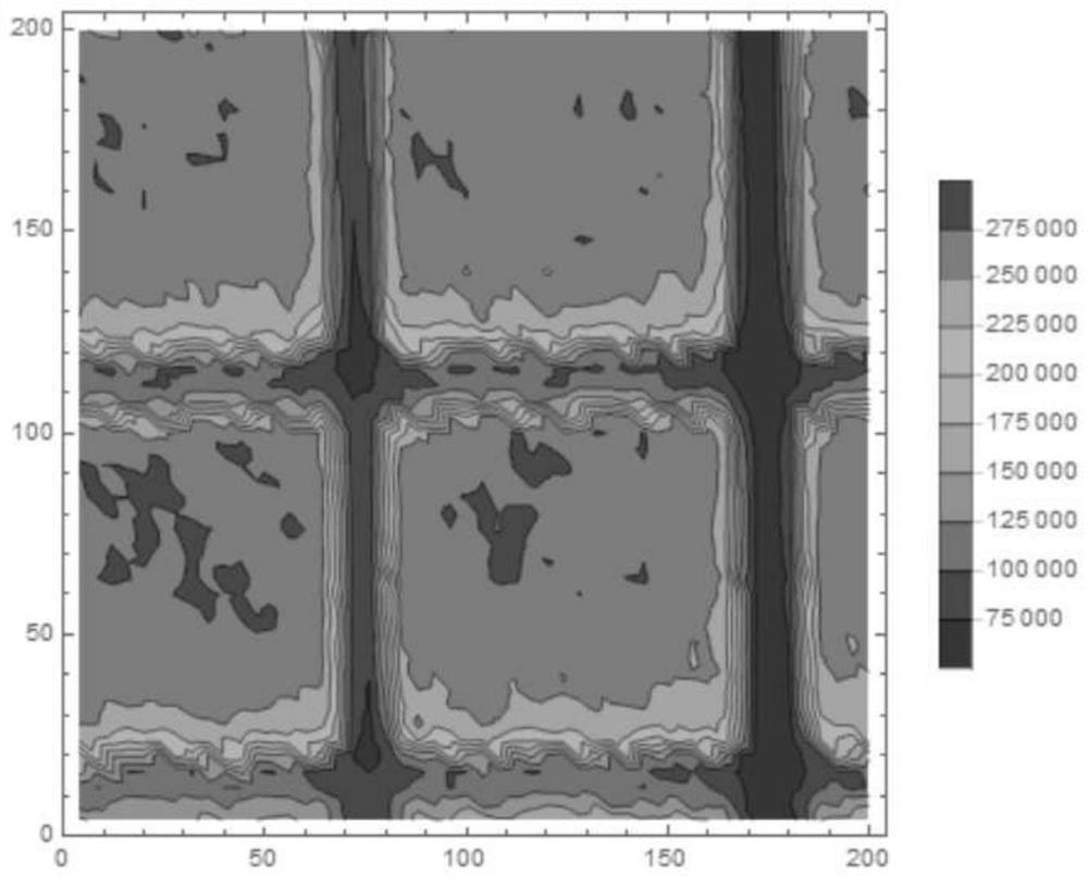
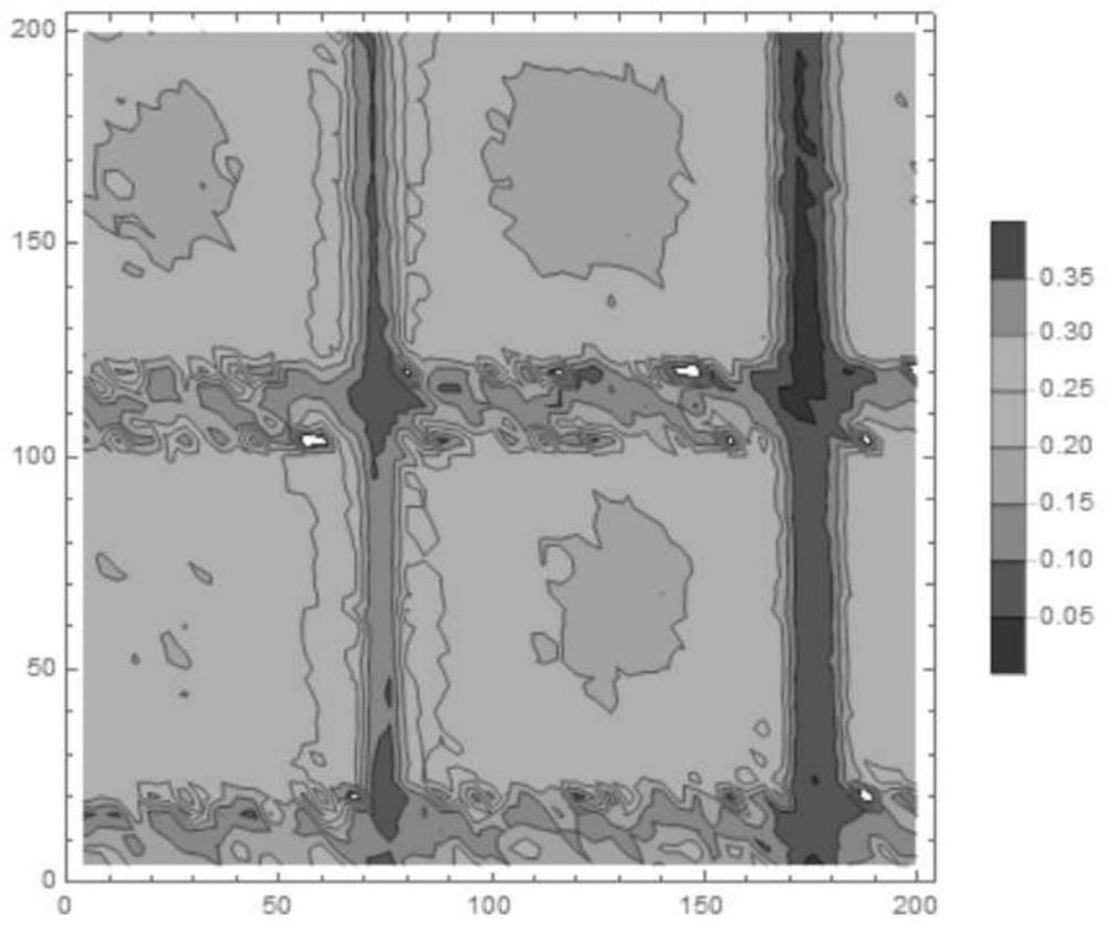
[0061]The silicon photomultiplier tube 10 detector is fixed on the nano-shift stage 2, and the silicon photomultiplier tube 10 ...


PUM


Abstract

The invention discloses a method for measuring PDE and Pct spatial two-dimensional distribution of a silicon photomultiplier. The method comprises the following steps: placing the silicon photomultiplier in an electromagnetic shielding box, and installing the silicon photomultiplier on a nanometer displacement platform; using a picosecond pulse laser driver to enable a laser head to irradiate picosecond laser beams, and focusing the picosecond laser beams into light spots on the surface of the silicon photomultiplier through a pinhole light-transmitting sheet in the microscope; powering the silicon photomultiplier by a stabilized power supply, amplifying an output avalanche pulse signal by a high-speed low-noise amplifier, and then inputting the amplified signal into a digital oscilloscopeto observe the waveform of the avalanche pulse; and controlling a nano displacement table to move, calculating a group of PDE and Pct at each position through the total pulse counting rate and the background counting rate under different photon equivalent thresholds, and finally drawing a spatial two-dimensional distribution diagram through multiple groups of PDE and Pct data. The relative lightdetection efficiency and optical crosstalk probability spatial two-dimensional distribution information of the silicon photomultiplier can be obtained at room temperature without low-temperature refrigeration.

Description

technical field [0001] The invention belongs to the technical field of weak light detection methods, and in particular relates to a method for measuring the two-dimensional distribution of PDE and Pct space of a silicon photomultiplier tube. Background technique [0002] Silicon photomultiplier (SiPM) is composed of hundreds to tens of thousands of avalanche photodiode (APD) cell arrays with a diameter of several to tens of microns integrated on the same single crystal silicon wafer. It is used in nuclear physics, medical imaging, laser Ranging (LIDAR), biophysics, quantum optics, quantum informatics and other fields have a wide range of applications. High-performance SiPM is the foundation of the above applications. Developing SiPMs with high photon detection efficiency (PD E), low optical crosstalk probability (Pct), low dark count rate (DCR) and post-pulse probability has become the goal of developers. At present, there have been many works on improving SiPM performance...

Claims


Application Information

Patent Timeline
Patent Type & Authority Applications(China)
IPC IPC(8): G01R31/25
CPCG01R31/252
Inventor 张国青张晨曹馨悦刘丽娜杨亚贤
Owner XI'AN POLYTECHNIC UNIVERSITY
Why Eureka
Try Eureka