MOS transistor and manufacturing process thereof

A MOS transistor and manufacturing process technology, which is applied in the field of MOS transistors and its manufacturing process, can solve the problems of poor electrical characteristics of finished transistors, poor device withstand voltage capability, and difficult transistor refinement, so as to reduce built-in resistance and gate Capacitance, improve the effect of voltage tolerance

Pending Publication Date: 2021-03-09
深圳宝铭微电子有限公司
View PDF4 Cites 0 Cited by
  • Summary
  • Abstract
  • Description
  • Claims
  • Application Information

AI Technical Summary

Problems solved by technology

[0003] Most MOS transistors are P-type MOS tubes, and the current moves along the horizontal direction of the surface. The finished device has poor withstand voltage capability, and it is difficult to reduce the gate capacitance. Moreover, the existing MOS transistor manufacturing process has few links, and it is difficult to refine the transistor. , it is difficult to strictly control the quality of the manufacturing process, and the electrical characteristics of the finished transistor are poor

Method used


Image

  • MOS transistor and manufacturing process thereof
  • MOS transistor and manufacturing process thereof

Examples


Embodiment Construction

[0036] The following will clearly and completely describe the technical solutions in the embodiments of the present invention with reference to the accompanying drawings in the embodiments of the present invention. Obviously, the described embodiments are only some, not all, embodiments of the present invention. Based on the embodiments of the present invention, all other embodiments obtained by persons of ordinary skill in the art without making creative efforts belong to the protection scope of the present invention.

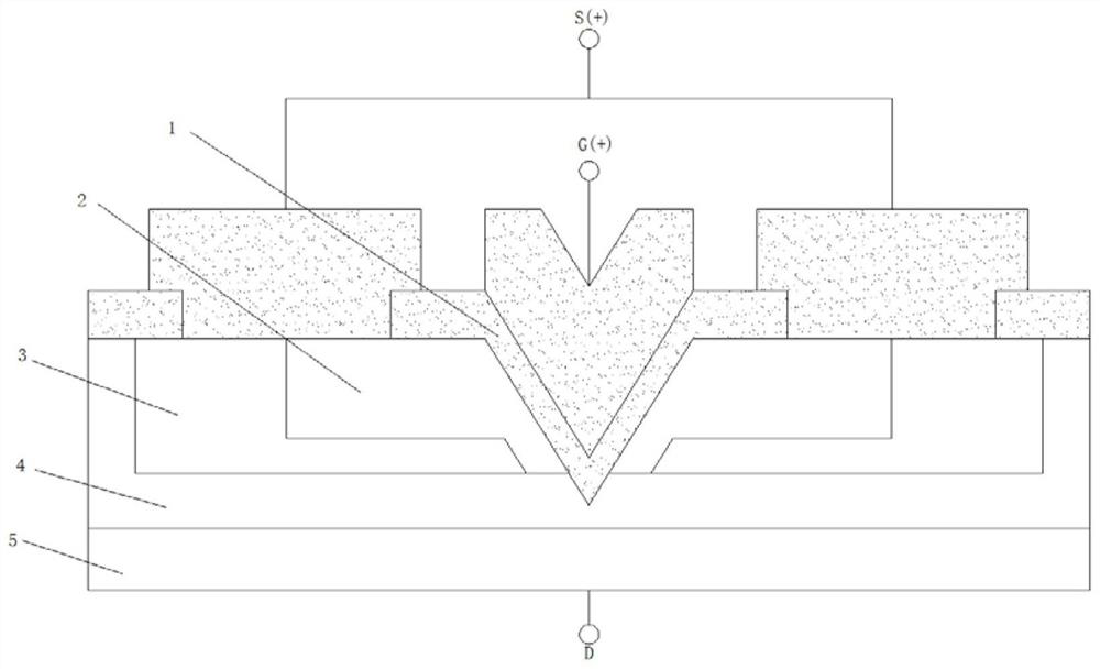
[0037] refer to Figure 1-2 , a MOS transistor and its manufacturing process, including an n-type channel 1, the length of the n-type channel 1 is one to two microns, the top surface of the n-type channel 1 is fixedly connected with a V-shaped groove 6, and the material of the V-shaped groove 6 It is polysilicon, the groove wall of the V-shaped groove 6 is 54.7 degrees to the plane of the silicon wafer, and the left and right sides of the n-type channel 1 are ...


PUM

PropertyMeasurementUnit
thicknessaaaaaaaaaa

Abstract

The invention discloses an MOS transistor and a manufacturing process thereof. The MOS transistor comprises an n-type channel, wherein the top surface of the n-type channel is fixedly connected with aV-shaped groove, the left side and the right side of the n-type channel are each provided with an N+ diffusion source region, the bottom of each N+ diffusion source region is connected with a p-channel body region, the bottom of each p-channel body region is connected with an N- drift region, and the bottom of each N- drift region is connected with an N+ substrate. The method comprises the following steps: S1, cutting a prepared substrate original silicon wafer into a circular sheet-shaped structure. The limit voltage of the device is effectively improved, the effect of conveniently reducingthe gate capacitance is achieved, the overall packaging density of the chip is effectively improved, the voltage endurance capacity of the device is improved, the purity of the transistor is effectively improved, and the purpose of conveniently and separately controlling the technology of each link is achieved; the effect of conveniently refining the transistor is achieved, the transistor manufacturing process quality is effectively improved, and the electrical property of a finished transistor device is improved.

Description

technical field [0001] The invention relates to the technical field of MOS transistors, in particular to a MOS transistor and a manufacturing process thereof. Background technique [0002] The full name of MOS transistors is metal oxide semiconductor field effect transistors, which can be divided into two categories: N-channel and P-channel. P-channel silicon MOS field-effect transistors have two P+ regions on the N-type silicon substrate, which are called sources. and the drain, there is no conduction between the two poles, and when sufficient positive voltage is applied to the source (the gate is grounded), the N-type silicon surface under the gate presents a P-type inversion layer, which becomes a channel connecting the source and drain road. Changing the gate voltage can change the hole density in the channel, thus changing the resistance of the channel. [0003] Most MOS transistors are P-type MOS tubes, and the current moves along the horizontal direction of the surf...

Claims


Application Information

Patent Timeline
Patent Type & Authority Applications(China)
IPC IPC(8): H01L21/336H01L29/423
CPCH01L29/66666H01L29/4236
Inventor 黄亚军黎忠瑾
Owner 深圳宝铭微电子有限公司
Why Eureka
Try Eureka