Three-dimensional intelligent micro-system chip

A microsystem and chip technology, which is applied in the components of TV systems, microstructure technology, microstructure devices, etc., can solve the difficult wafer-wafer three-dimensional integration process, increase the difficulty of intelligent microsystems, and difficult to integrate traditional sensors, etc. problems, to achieve the effect of improving R&D efficiency, lowering test costs, and reducing chip area

Active Publication Date: 2021-03-30
SHANGHAI INST OF MICROSYSTEM & INFORMATION TECH CHINESE ACAD OF SCI
View PDF10 Cites 1 Cited by
  • Summary
  • Abstract
  • Description
  • Claims
  • Application Information

AI Technical Summary

Problems solved by technology

However, the discrete architecture and board-level wires limit the speed of data transmission, and the separation of the sensor from the chip leads to defects such as low integration, high testing costs, and poor robustness.
At the same time, due to the high manufacturing temperature (greater than 1000 degrees Celsius), traditional sensors (such as MEMS) are difficult to integrate with CMOS, and additional processes such as epitaxy are required
The sampling area of ​​the sensor must be exposed in front of the object to be measured, and it is difficult to simply adopt the wafer-wafer 3D integration process
The data collected by the sensor is raw data, which must be processed and calculated by analog circuits and processors, which increases the difficulty of designing intelligent microsystems

Method used


Image

  • Three-dimensional intelligent micro-system chip
  • Three-dimensional intelligent micro-system chip
  • Three-dimensional intelligent micro-system chip

Examples


Embodiment 1

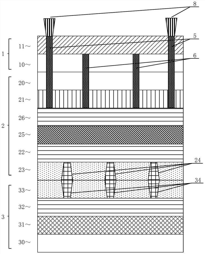
[0057] figure 1 A schematic structural diagram of a hierarchical storage scheme (new type) of a three-dimensional intelligent microsystem chip provided in this embodiment, the chip includes:

[0058] The first chip 1; including a first sensing layer 11 and a fourth substrate 10; the fourth substrate 10 is stacked on the first sensing layer 11;

[0059] The second chip 2; includes a first substrate 20, a first active region layer 21, a first metal layer 22, a first dielectric layer 23 and a first through hole 24; wherein, the number of the first through hole 24 can be One, or multiple; the first substrate 20, the first active region layer 21, the first metal layer 22 and the first dielectric layer 23 are sequentially stacked and connected, and the first through hole 24 is provided in the first dielectric layer 23, the first through hole 24 connects the first metal layer 22 and the outside of the first dielectric layer 23, and the first through hole 24 is the input end or outp...

Embodiment 2

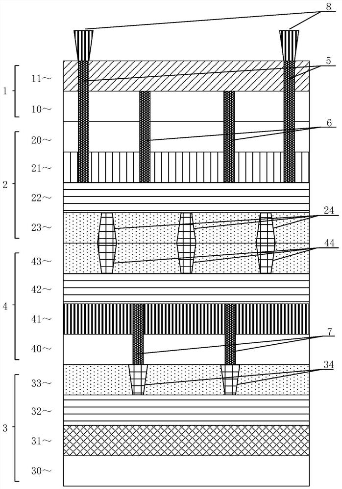
[0067] figure 2 A schematic diagram of a hierarchical storage scheme (traditional) structure of a three-dimensional intelligent microsystem chip provided in this embodiment, the chip includes:

[0068] The first chip 1; including a first sensing layer 11 and a fourth substrate 10; the fourth substrate 10 is stacked on the first sensing layer 11;

[0069] The second chip 2; includes a first substrate 20, a first active region layer 21, a first metal layer 22, a first dielectric layer 23 and a first through hole 24; wherein, the number of the first through hole 24 can be One, or multiple; the first substrate 20, the first active region layer 21, the first metal layer 22 and the first dielectric layer 23 are sequentially stacked and connected, and the first through hole 24 is provided in the first dielectric layer 23, the first through hole 24 connects the first metal layer 22 and the outside of the first dielectric layer 23, and the first through hole 24 is the input end or ou...


PUM


Abstract

The invention relates to a three-dimensional intelligent micro-system chip. The three-dimensional intelligent micro-system chip mainly comprises a first chip, a second chip and a third chip, wherein the first chip comprises a sensing layer. Aiming at the problem that a traditional sensor (such as an MEMS) is difficult to integrate with a CMOS, according to the three-dimensional intelligent micro-system chip, the sensor, a processor and a memory can achieve higher integration density and better robustness through the wafer-level integrated packaging, the parasitic capacitance in electrical connection is reduced, the test cost is reduced, the three-dimensional intelligent micro-system chip is the premise for achieving a large-array sensor, and the risk that the data is stolen is also reducedbecause of the internal transmission of the data. Meanwhile, the advantages of better material compatibility and faster product development period of a multi-chip scheme are kept.

Description

technical field [0001] The invention belongs to the field of integrated circuits, in particular to a three-dimensional intelligent microsystem chip. Background technique [0002] In a general sense, intelligent microsystems refer to the guidance of the theory of miniaturization, systematization, and intelligence, adopting new architectural ideas and design methods at the levels of material domain, information domain, and energy domain, through three-dimensional / heterogeneous / Heterogeneous integration and other advanced manufacturing methods form a miniaturized system device with a characteristic scale of micro-nano level, which has multiple functions such as information acquisition, processing, communication, execution, and energy supply, and can work independently and intelligently. It is an intelligent microsystem unit or an intelligent microsystem node. Under traditional microsystems or classic computer architectures, sensing, storage, and computing are discrete, reflec...

Claims


Application Information

Patent Timeline
Patent Type & Authority Applications(China)
IPC IPC(8): H01L23/50H01L23/52H01L25/18B81B7/00B81B7/02G01D21/02
CPCH01L25/18H01L23/50H01L23/52B81B7/02B81B7/0006G01D21/02Y02D10/00
Inventor 雷宇张光明刘梦陈后鹏宋志棠
Owner SHANGHAI INST OF MICROSYSTEM & INFORMATION TECH CHINESE ACAD OF SCI
Why Eureka
Try Eureka