A method for preparing the back of a perc single crystal double-sided solar cell

A technology on the back of solar cells, applied in circuits, electrical components, photovoltaic power generation, etc., can solve the problems of silicon substrate damage, increase laser energy consumption, affect the electrical performance of solar cells, etc., achieve the effect of reducing recombination centers and improving conversion efficiency

Active Publication Date: 2022-08-09
JETION SOLAR HLDG
View PDF0 Cites 0 Cited by
  • Summary
  • Abstract
  • Description
  • Claims
  • Application Information

AI Technical Summary

Problems solved by technology

This method must use a high-energy laser to irradiate the silicon substrate to remove the laminated passivation dielectric film deposited on a specific area on the back, so the silicon substrate will inevitably be damaged during the laser ablation process, thereby causing damage to the silicon substrate surface and the silicon substrate. Defects occur in the substrate body, which affects the electrical properties of the solar cell. In addition, when high laser energy is used for ablation, the energy consumption of the laser is bound to increase, thereby increasing the manufacturing cost of the back of the solar cell.

Method used


Image

  • A method for preparing the back of a perc single crystal double-sided solar cell
  • A method for preparing the back of a perc single crystal double-sided solar cell

Examples


Embodiment 1

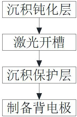
[0025] like figure 1 As shown, the method for preparing the back surface of the PERC single crystal double-sided solar cell of Example 1 includes the following steps:

[0026] (1) Deposition of passivation layer: ALD (atomic layer deposition) method is used to deposit an aluminum oxide film on the back of the polished silicon substrate. The thickness of the aluminum oxide film is 6nm, the refractive index is 1.65, the deposition temperature is 300°C, and the deposition time is 300°C. is 35s, and the deposition pressure is 1000pa;

[0027] (2) Laser grooving: use a low-energy laser to irradiate the aluminum oxide film on the back of the silicon substrate to form a grooved area on the surface of the aluminum oxide to expose the silicon substrate in the grooved area, where the laser power is 10W and the laser frequency is 1200kHz , the laser speed is 35000m / s, and the laser spot diameter is 25um;

[0028] (3) Deposition of protective layer: use PECVD (plasma vapor deposition) m...

Embodiment 2

[0031] The method for preparing the backside of the PERC single crystal double-sided solar cell of Example 2 is based on Example 1, with the difference that the laser speed in step (2) is increased, the laser power is reduced, and the laser spot diameter is reduced, that is, the following steps are included:

[0032] (1) Deposition of passivation layer: ALD (atomic layer deposition) method is used to deposit an aluminum oxide film on the back of the polished silicon substrate. The thickness of the aluminum oxide film is 6nm, the refractive index is 1.65, the deposition temperature is 300°C, and the deposition time is 300°C. is 35s, and the deposition pressure is 1000pa;

[0033] (2) Laser grooving: use a low-energy laser to irradiate the aluminum oxide film on the back of the above silicon substrate, form a grooved area on the surface of the aluminum oxide, and expose the silicon substrate in the grooved area, where the laser power is 8W and the laser frequency is 1200kHz , th...

Embodiment 3

[0037] The method for preparing the back surface of the PERC single crystal double-sided solar cell in Example 3 is based on Example 1, except that the deposition time in step (3) is extended to increase the thickness of the silicon nitride film, that is, the following steps are included:

[0038] (1) Deposition of passivation layer: ALD (atomic layer deposition) method is used to deposit an aluminum oxide film on the back of the polished silicon substrate. The thickness of the aluminum oxide film is 6nm, the refractive index is 1.65, the deposition temperature is 300°C, and the deposition time is 300°C. is 35s, and the deposition pressure is 1000pa;

[0039] (2) Laser grooving: use a low-energy laser to irradiate the aluminum oxide film on the back of the silicon substrate to form a grooved area on the surface of the aluminum oxide to expose the silicon substrate in the grooved area, where the laser power is 10W and the laser frequency is 1200kHz , the laser speed is 35000m / s...


PUM

PropertyMeasurementUnit
thicknessaaaaaaaaaa
thicknessaaaaaaaaaa
thicknessaaaaaaaaaa

Abstract

The invention discloses a method for preparing the back surface of a PERC single crystal double-sided solar cell, comprising the following steps: S1, depositing a passivation layer on the back surface of a silicon substrate; S2, using a low-energy laser to irradiate the passivation layer with laser light, so that the laser irradiates the passivation layer with laser light. The lower passivation layer forms a groove, and the silicon substrate in the groove is exposed; S3, deposit a protective layer on the surface of the groove and the passivation layer, and the protective layer is a silicon nitride film; S4, use electronic paste to burn through the groove The protective layer is prepared, and the back electrode is in contact with the silicon substrate in the groove. In the method for preparing the back of the PERC single crystal double-sided solar cell, immediately after depositing the passivation layer, a low-energy laser is used for grooving, which reduces damage to the silicon substrate and reduces energy consumption, and then deposits a protective layer, which not only realizes the protection of the passivation layer It also has a repairing effect on the surface of the silicon substrate and in the body, reducing the recombination center and improving the conversion efficiency of the battery.

Description

technical field [0001] The invention relates to the technical field of backside preparation of PERC cells, in particular to a method for preparing the backside of a PERC single crystal double-sided solar cell. Background technique [0002] PERC technology is to add a passivation layer (alumina or silicon oxide) on the back of the silicon wafer to passivate the silicon wafer, which can effectively improve the minority carrier lifetime. In order to prevent the passivation layer from being damaged and affecting the passivation effect, a protective layer (silicon nitride) is also plated on the outside of the passivation layer. Since the passivation layer is an insulating layer, it cannot form an electrode path with the aluminum back field. Therefore, it is necessary to groove the back side of the silicon wafer by laser to expose the silicon substrate and form the local surface field of the PERC monocrystalline silicon solar cell. [0003] At present, the production process of t...

Claims


Application Information

Patent Timeline
Patent Type & Authority Patents(China)
IPC IPC(8): H01L31/18H01L31/068H01L31/0224
CPCH01L31/1804H01L31/1868H01L31/068H01L31/022441Y02P70/50
Inventor 康海涛胡燕曹思远郭万武
Owner JETION SOLAR HLDG
Why Eureka
Try Eureka