Silicon carbide single crystal wafer and method for producing silicon carbide single crystal ingot

A technology of silicon carbide single crystal and manufacturing method, applied in chemical instruments and methods, single crystal growth, single crystal growth and other directions, can solve the problems of unfavorable investment budget and time, indistinguishable, etc., and achieve less dislocation and dislocation. Evenly distributed effect

Pending Publication Date: 2021-04-09
CENTRAL RESEARCH INSTITUTE OF ELECTRIC POWER INDUSTRY +1
View PDF7 Cites 0 Cited by
  • Summary
  • Abstract
  • Description
  • Claims
  • Application Information

AI Technical Summary

Problems solved by technology

In addition, in the process of manufacturing components, when there is a deviation in the in-plane area in terms of the yield of component products, if the current wafer is used, it is impossible to distinguish whether it is caused by the process or caused by the wafer, so that the process improvement will be long-term, resulting in Unfavorable in terms of budget and time invested, which is also a current issue

Method used


Image

  • Silicon carbide single crystal wafer and method for producing silicon carbide single crystal ingot
  • Silicon carbide single crystal wafer and method for producing silicon carbide single crystal ingot
  • Silicon carbide single crystal wafer and method for producing silicon carbide single crystal ingot

Examples


Embodiment 1

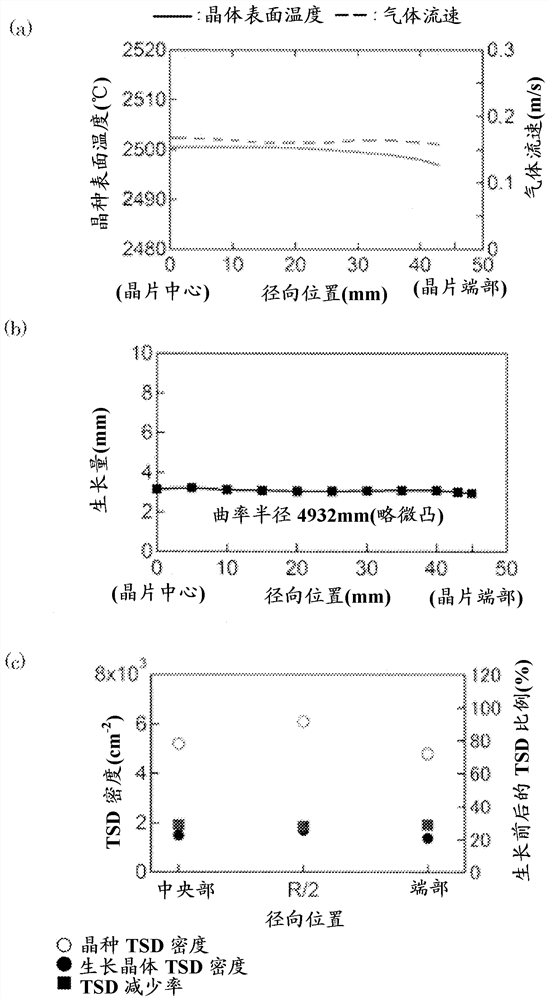
[0099] If so Figure 6 The surface temperature of the seed crystal shown in (a) (a temperature gradient of about 0.06°C / mm) and the flow rate of the source gas allow the SiC single crystal 51 to grow, as Figure 6 As shown in (b), a SiC single crystal with a radius of curvature of 4932 mm and slightly convex (slightly convex) was obtained. The internal stress of a single crystal can be determined by image 3 It is estimated to be below 10Mpa.

[0100] The TSD densities at the center, end, and middle (1 / 2 of the radius R) of the SiC single crystal were measured. show the result in Figure 6 (c).

[0101] As a result, no matter where it is placed, the TSD density is 2000 / cm 2 Below, almost the same number, relative to 5000 seed crystals / cm 2 ~6000pcs / cm 2 , reduced by about 30%, and the distribution is evened out.

Embodiment 2

[0107] exist Figure 8 Example 2 is shown. The figure is the result of investigating the dislocation density in the crystal grown by the gas method (2.5 mm growth position) and in the seed crystal. It can be seen that the seed crystal is a crystal grown by the usual growth method, that is, the sublimation method, and the dislocation density distribution is relatively large in the crystal plane. On the other hand, it can be seen that in the crystal grown to 2.5 mm by the gas method, the dislocation density is greatly reduced, and the dislocation density has little uniform variation regardless of the site in the crystal plane. From this result, it is also clear from the examples that the distribution of dislocations becomes uniform in the crystal grown by the gas method.


PUM


Abstract

Provided are a method for producing a silicon carbide single crystal wafer, which is capable of obtaining a high-grade silicon carbide single crystal; and a silicon carbide single crystal wafer. A silicon carbide single crystal wafer produced by a vapor phase growth method is characterized in that the dislocation density contained in the wafer is 3500 pieces / cm2 or less, and the difference in the density of the KOH pits is less than 50% of the average value in the comparison of the center portion of the wafer, the end portions of the wfer, and the middle portion of the wafer.

Description

technical field [0001] The invention relates to a method for manufacturing a silicon carbide single crystal wafer and a silicon carbide single crystal ingot. Background technique [0002] Silicon carbide (hereinafter also referred to as SiC) has excellent physical properties of about 3 times the band gap, about 2 times the saturation drift speed, and about 10 times the insulation breakdown field strength compared with Si, and has a larger thermal conductivity. High-efficiency semiconductors, and thus are expected to be used as materials for realizing next-generation high-voltage / low-loss semiconductor elements that greatly exceed the performance of Si single-crystal semiconductors currently used. [0003] Currently, a sublimation method is used as one of methods for producing commercially available silicon carbide single crystals. [0004] Most of the currently commercially available silicon carbide single crystal wafers are produced by the sublimation method, but the subli...

Claims


Application Information

Patent Timeline
IPC IPC(8): C30B29/36C30B25/00
CPCC30B29/36C30B25/00C30B25/10C30B33/00C30B25/02
Inventor 镰田功穗土田秀一星乃纪博德田雄一郎冈本武志
Owner CENTRAL RESEARCH INSTITUTE OF ELECTRIC POWER INDUSTRY
Why Eureka
Try Eureka