A High Resolution Spectrometer Based on Euler Microring Resonator
A micro-ring resonant cavity and high-resolution technology, applied in the field of on-chip spectrometers, achieves the effects of plug and play, extended working bandwidth, and complete structure
- Summary
- Abstract
- Description
- Claims
- Application Information
AI Technical Summary
Problems solved by technology
Method used
Image
Examples
specific Embodiment
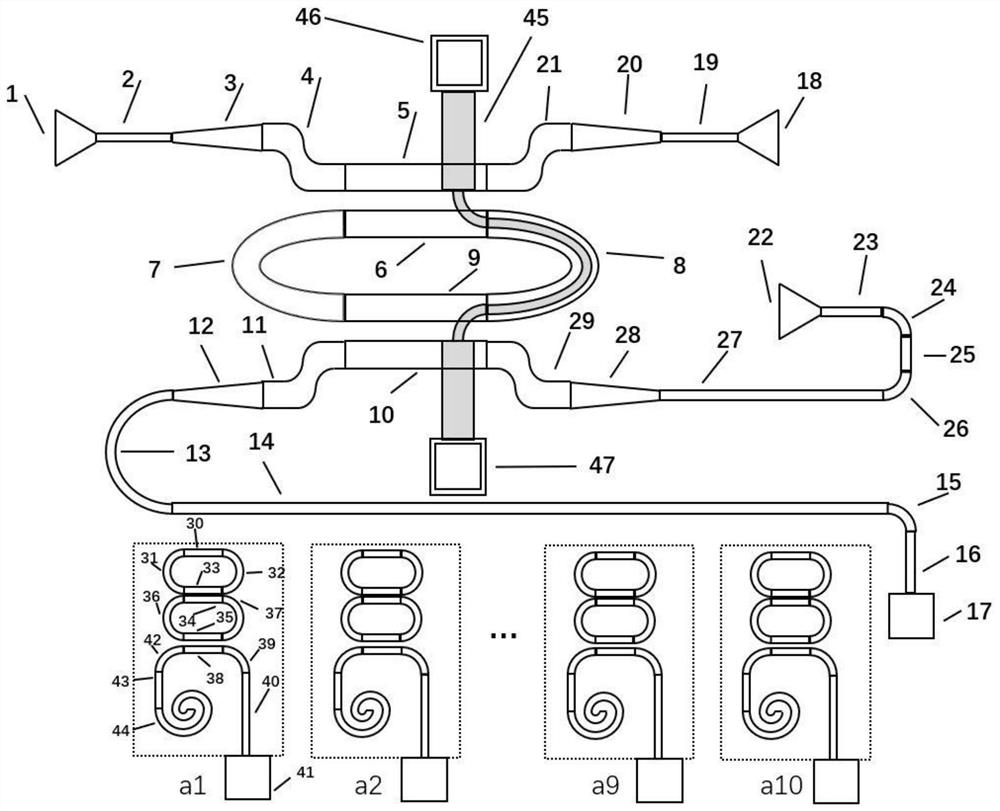
[0059] The silicon nanowire optical waveguide based on silicon insulator (SOI) material is selected: the core layer is silicon material, the thickness is 220nm, and the refractive index is 3.4744; the lower cladding material is SiO2, the thickness is 2μm, and the refractive index is 1.4404; The cladding material is SiO2, the thickness is 1.5μm, and the refractive index is 1.4404; the metal material of the heating electrode is titanium gold.
[0060] The width of the first single-mode waveguide 2 is 420nm, and the length is 100μm. For the tapered waveguides 3, 20, 12, 28, the width of the narrow waveguide is 420nm, and the width of the wide waveguide is 1600nm, and the length is 30μm. Therefore, the introduction of a wide waveguide can greatly reduce the transmission loss of the waveguide and improve the resolution of the spectrometer. The S-shaped curved waveguides 4, 21, 11, and 29 have a lateral width of 40 μm, a longitudinal length of 0.5 μm, and a width of both input and o...
PUM
 Abstract
Description
Claims
Application Information


