Edge-doped crystalline silicon solar cell structure and production method thereof

A solar cell and edge technology, applied in the field of solar cells, can solve problems such as no good solution

Pending Publication Date: 2021-04-20
TRINA SOLAR CO LTD
View PDF11 Cites 0 Cited by
  • Summary
  • Abstract
  • Description
  • Claims
  • Application Information

AI Technical Summary

Problems solved by technology

[0003] At present, the industry does not have a good sol...

Method used


Image

  • Edge-doped crystalline silicon solar cell structure and production method thereof
  • Edge-doped crystalline silicon solar cell structure and production method thereof
  • Edge-doped crystalline silicon solar cell structure and production method thereof

Examples


Embodiment 1

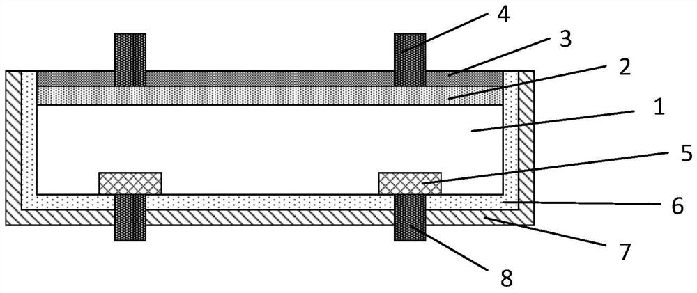
[0041] In order to solve the above problems, the present invention provides a crystalline silicon solar cell structure capable of reducing laser cutting edge loss and a preparation method thereof. For clarification, the present invention still uses figure 1 The p-type PERC battery is used as an example, but those skilled in the art can understand that the present invention is also suitable for n-type PERC batteries. According to the first embodiment of the present invention, as Figure 5 As shown, in the area to be cut by the laser (near the midline in the example of half cutting), the solid dopant source 9 is printed on the front side of the cell by screen printing. In one example, the dopant source 9 may be phosphorous. Alternatively, the dopant source can also be other materials suitable for heavily doping the edges, such as boron, gallium or a combination of these materials.

[0042] Subsequently, the solid dopant source 9 is irradiated with laser light. In one example...

Embodiment 2

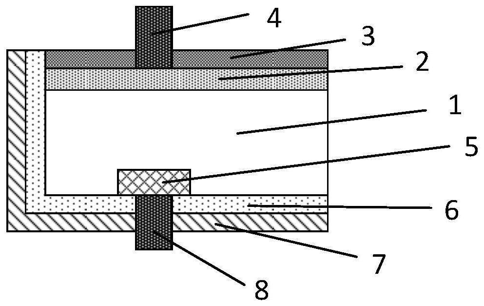
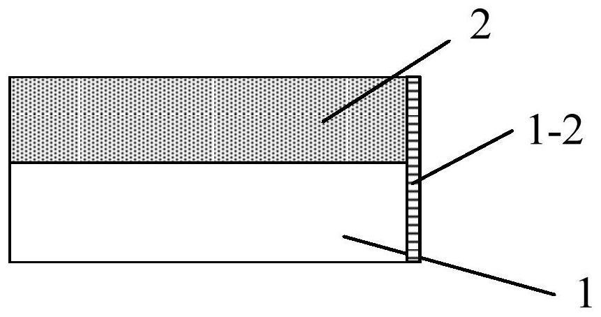
[0048] For clarification, the figure 1 Taking the p-type PERC battery as an example, according to the second embodiment of the present invention, the battery structure is firstly cut by laser, and after the laser cutting is completed, a half-sheet battery ( figure 2 ). Subsequently, by screen printing, a solid dopant source 9 (such as Figure 7 shown), and then irradiate the solid dopant source 9 with a laser, the laser generates heat, and the dopant atoms are doped into the silicon wafer 1, forming an edge heavily doped region 13 (such as Figure 9 shown). At this time, it turns out image 3 The 1-2 edge part in is heavily doped, and for this side p-n junction, the center of the junction region is moved from the original 1-2 to Figure 9 The interface between the middle silicon wafer 1 and the edge emitter 13 is far away from the laser-cut interface 1-2, thus reducing the influence of the region 1-2 on the overall recombination.

[0049] Alternatively or additionally, a...


PUM

PropertyMeasurementUnit
Thicknessaaaaaaaaaa
Thicknessaaaaaaaaaa

Abstract

The invention provides an edge-doped crystalline silicon solar cell structure and a production method thereof. A heavily doped region is arranged on each laser cutting edge interface of a solar cell to reduce the concentration of minority carriers reaching the edge interface so as to inhibit edge recombination. A passivation film can be further arranged on the surface of the edge heavily doped region to enhance surface passivation, field passivation and chemical passivation of an edge interface are formed, the composite current density of the edge is reduced, and the open-circuit voltage of the battery is improved.

Description

technical field [0001] The invention relates to the technical field of solar cells, and more particularly, relates to a structure and a preparation method of an edge-doped crystalline silicon solar cell. Background technique [0002] At present, due to the popularization of cutting half-cell components, shingling technology, merging and splicing technology, the use of laser to cut the whole battery cell has gradually become the mainstream trend of the industry. Especially for the promotion and application of large silicon wafers, cutting the whole battery into 1 / 2, 1 / 3,...1 / n to reduce the series resistance of the module is the only way to increase the output power of the module. However, at present, the industry has found in practice that when the laser cuts the battery sheet, the section generated by laser ablation interface and thermal stress or mechanical stress to separate the battery, due to the existence of a large number of dangling bonds and defect states on the sur...

Claims


Application Information

Patent Timeline
IPC IPC(8): H01L31/0224H01L31/0216H01L31/06H01L31/18
CPCY02E10/50Y02P70/50
Inventor 陈奕峰陈达明刘成法邹扬王尧龚剑冯志强高纪凡
Owner TRINA SOLAR CO LTD
Why Eureka
Try Eureka