

Silicon wafer cutting machine
A cutting machine, silicon wafer technology, applied in conveyor objects, laser welding equipment, transportation and packaging, etc., can solve problems such as low work efficiency, shutdown operation, etc., to improve the cutting effect, ensure the fineness, and improve the processing effect. Effect
- Summary
- Abstract
- Description
- Claims
- Application Information
AI Technical Summary
Problems solved by technology
Method used
Image

Examples
Embodiment Construction
[0023] The following will clearly and completely describe the technical solutions in the embodiments of the present invention with reference to the accompanying drawings in the embodiments of the present invention. Obviously, the described embodiments are only some, not all, embodiments of the present invention. Based on the embodiments of the present invention, all other embodiments obtained by persons of ordinary skill in the art without making creative efforts belong to the protection scope of the present invention.
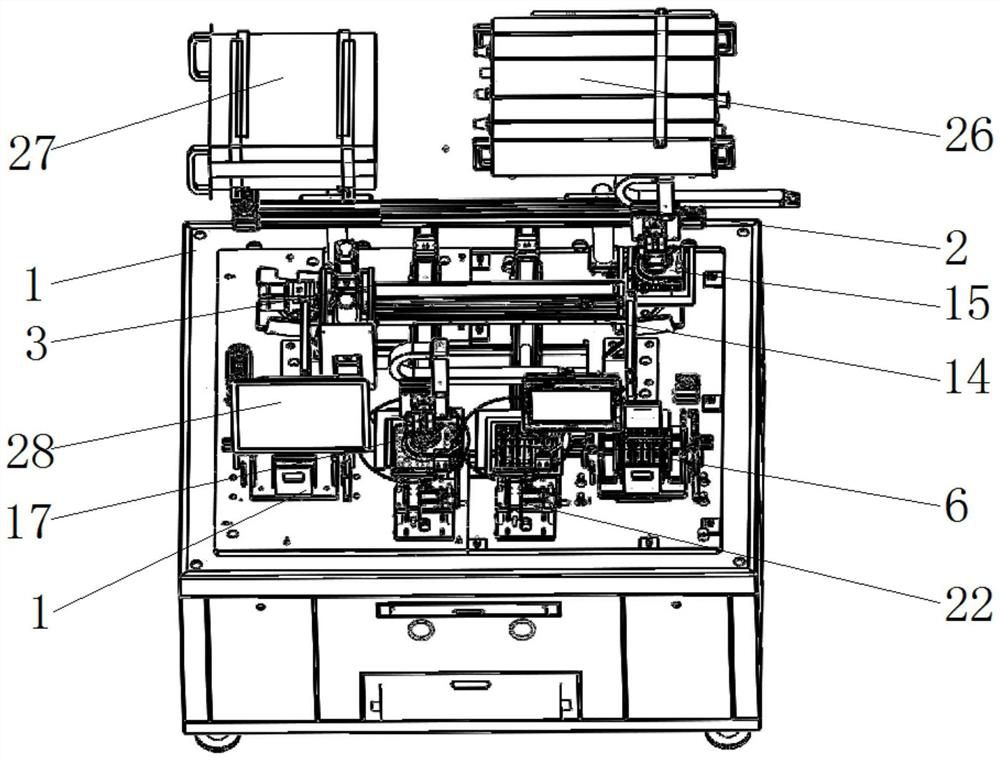
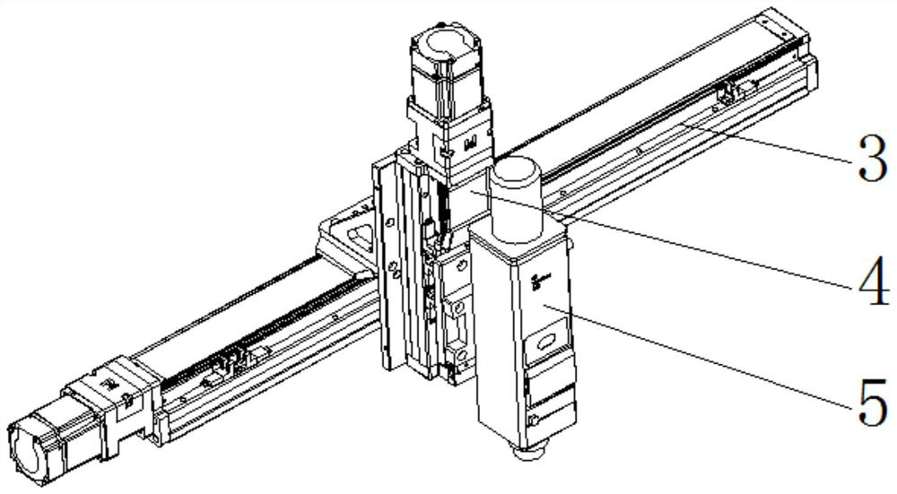
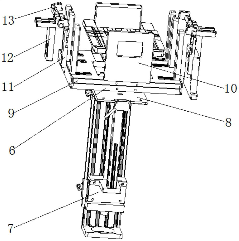
[0024] see Figure 1-6 , the present invention provides a technical solution: a silicon wafer cutting machine, including a body 1, a motion module 2, a cutting module 3, an optical fiber laser integrated 4, a laser cutting head 5, a first material box 6, a lifting lower Block 7, jacking upper block 8, material box cushion block 9, material box rib 10, opposite shot column 11, support frame 12, blowing block 13, movement frame 14, second material box 15, finish...
PUM
 Abstract
Description
Claims
Application Information