Wax-free polishing method for ultrathin semiconductor wafer

A semiconductor and wafer technology, applied in the field of semiconductor preparation, can solve the problems of difficult infiltration of supply liquid, high fragmentation rate, high fragmentation rate, etc., and achieve the effects of weakening chlorine oxidation, not easy to float, and small fragmentation rate

Inactive Publication Date: 2021-04-30
FIRST SEMICON MATERIALS
View PDF7 Cites 4 Cited by
  • Summary
  • Abstract
  • Description
  • Claims
  • Application Information

AI Technical Summary

Problems solved by technology

[0005] (1) Because the wafer is thin, there is a high probability of debris during the process of wax absorption under vacuum conditions in the chamber;
[0006] (2) Due to the difficulty in infiltrating the supply liquid during the polishing process, dry grinding will be caused during the polishing process, and the debris rate is high;
[0007] (3) The debris rate is also high during the waxing process
[0008] (4) For double-polished wafers, it needs to be waxed and roughly polished twice. The thinner the wafer, the higher the debris rate
[0009] According to statistics, the overall breakage rate of GaAs wafers polished to 100 μm by the above-mentioned wax polishing process is as high as 40% to 70%.

Method used


Image

  • Wax-free polishing method for ultrathin semiconductor wafer

Examples


Embodiment 1

[0034] The wax-free polishing method of a kind of ultra-thin semiconductor wafer as the embodiment of the present invention, described method comprises the following steps:

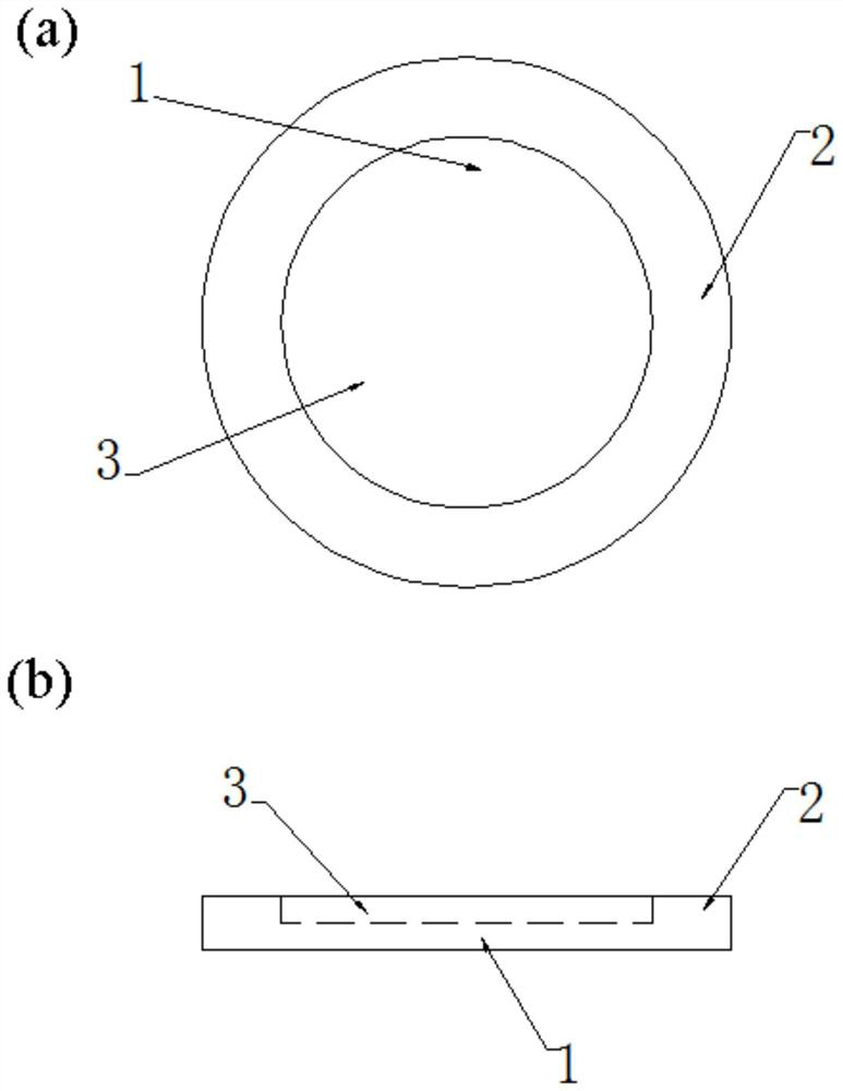
[0035] (1) Place the gallium arsenide wafer to be polished with a diameter of D on the adsorption pad mold A for rough back polishing, the adsorption pad mold A is provided with a round hole A, and the depth of the round hole A is 150-180 μm; The diameter of the circular hole A is (D+0.15)-(D+0.25) mm;

[0036] (2) Place the gallium arsenide wafer processed in step (1) on the adsorption pad mold B for rough polishing on the front side, the adsorption pad mold B is provided with a round hole B, and the depth of the round hole B is 120-150 μm ; The diameter of the circular hole B is (D+0.15)-(D+0.25) mm;

[0037] (3) Place the gallium arsenide wafer processed in step (2) on the adsorption pad mold C for back fine polishing, the adsorption pad mold C is provided with a circular hole C, and the depth of the ...

Embodiment 2

[0048] As a wax-free polishing method of an ultra-thin semiconductor wafer in an embodiment of the present invention, taking a 4-inch finished germanium sheet with a thickness of 135-155 μm and a diameter of 100 ± 0.05 mm as an example, the wax-free polishing method of an ultra-thin wafer in this embodiment is described in detail. instruction of.

[0049] The only difference between this embodiment and embodiment 1 is: (a), in the step (1), the flow rate of the polishing liquid for the rough polishing on the back is (78.5×9-50=650ml / min), the step In (2), the flow rate of the polishing fluid for the rough polishing on the front is (78.5×9-50=650ml / min), and in the step (3), the flow rate of the polishing fluid for the fine polishing on the back side is (78.5× 9-50=650ml / min), in the step (4), the flow rate of the polishing liquid for the fine polishing of the main surface is (2×78.5×9-50=1363ml / min).

[0050] The wax-free polishing method of the ultra-thin semiconductor wafer...


PUM

PropertyMeasurementUnit
depthaaaaaaaaaa
surface roughnessaaaaaaaaaa

Abstract

The invention provides a wax-free polishing method for an ultrathin semiconductor wafer, which comprises the following steps: (1) a gallium arsenide wafer to be polished with the diameter of D is placed on an adsorption pad mold A to be subjected to back rough polishing; the adsorption pad mold A is provided with a round hole A; the depth of the round hole A is 150-180 mu m; (2) the workpiece is placed on an adsorption pad mold B for front rough polishing; a round hole B is formed in an adsorption pad mold B; the depth of the round hole B ranges from 120 micrometers to 150 micrometers; (3) the gallium arsenide wafer processed in the step (2) is placed on an adsorption pad mold C to be subjected to back face fine polishing; the adsorption pad mold C is provided with a round hole C; the depth of the round hole C ranges from 80 micrometers to 120 micrometers; (4) placing the gallium arsenide wafer treated in the step (3) on the adsorption pad mold C for front fine polishing; and (5) washing. The wax-free polishing method for the ultrathin semiconductor wafer has the advantages that the breakage rate is lower; the percent of pass of the wax-free polishing double-polishing ultrathin gallium arsenide wafer processing technology is increased; and the production cost is reduced.

Description

technical field [0001] The invention relates to the field of semiconductor preparation, in particular to a wax-free polishing method for ultra-thin semiconductor wafers. Background technique [0002] As the second-generation semiconductor materials, gallium arsenide, germanium, etc., have shown more and more broad application prospects in the fields of mobile phones, infrared optics, and satellite communications by virtue of their superior electronic properties. However, in the production process from the growth of gallium arsenide crystal to the actual application of the finished gallium arsenide wafer, a series of complicated processing processes are required. Among them, during the polishing process of the ultra-thin gallium arsenide wafer, due to the thickness The fluctuation requirement range is narrow, generally 10-20μm; therefore, the flatness requirement is very high in the processing process, and the chip is thin, so the chipping rate is high in the processing proce...

Claims


Application Information

Patent Timeline
Patent Type & Authority Applications(China)
IPC IPC(8): B24B29/02B24B41/06B24B55/00
CPCB24B29/02B24B41/06B24B55/00
Inventor 肖进龙杨士超周铁军何剑辉
Owner FIRST SEMICON MATERIALS
Why Eureka
Try Eureka