Bridge chain type patterned sapphire substrate, preparation method and LED epitaxial wafer

A technology for patterning sapphire and sapphire substrates, which is used in semiconductor/solid-state device manufacturing, electrical components, circuits, etc. to increase the reflection area, increase the reflection interface area, and improve the reflection efficiency.

Pending Publication Date: 2021-05-04
广东中图半导体科技股份有限公司
View PDF6 Cites 0 Cited by
  • Summary
  • Abstract
  • Description
  • Claims
  • Application Information

AI Technical Summary

Problems solved by technology

However, with the rapid development of the LED display industry, the consumer market has higher and higher requirements for product quality and brightness. At present, LED chips with traditional micro-nano patterned sapphire substrates are difficult to meet the demand.

Method used


Image

  • Bridge chain type patterned sapphire substrate, preparation method and LED epitaxial wafer
  • Bridge chain type patterned sapphire substrate, preparation method and LED epitaxial wafer
  • Bridge chain type patterned sapphire substrate, preparation method and LED epitaxial wafer

Examples


Embodiment approach

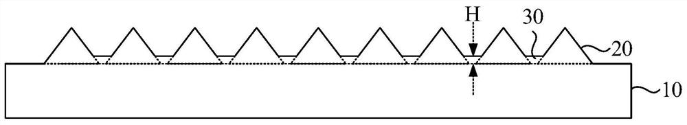
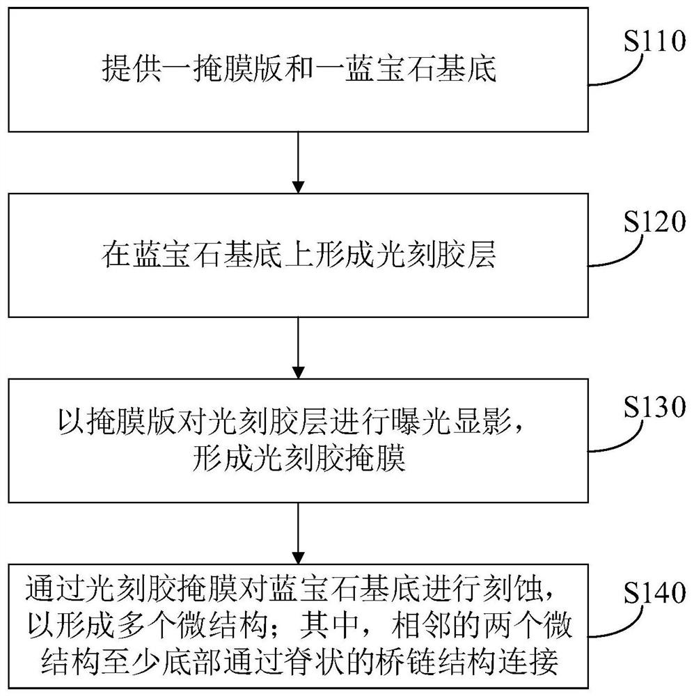
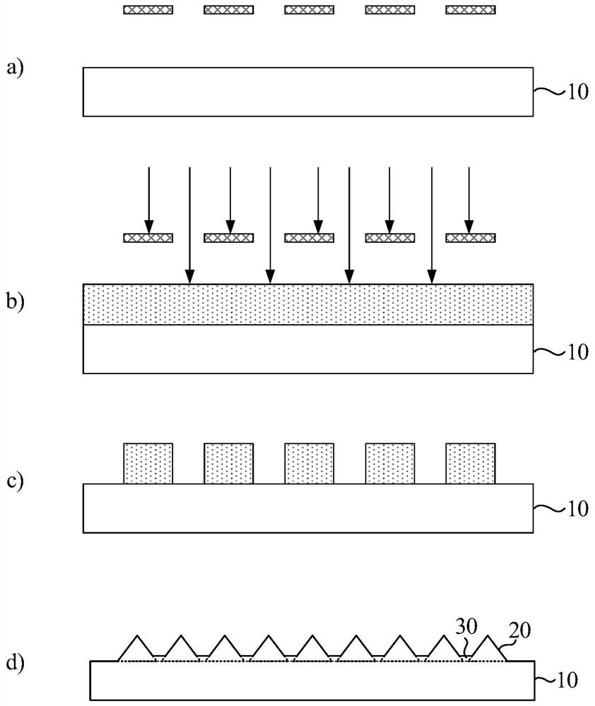
[0077] Based on the various implementation modes provided by the present invention, the bridge-chain patterned sapphire substrate and the preparation method of the present invention will be introduced below with a specific example. Figure 15 It is a cross-sectional SEM test diagram of a photoresist mask provided by an embodiment of the present invention under different magnifications, Figure 16 The embodiment of the present invention provides a cross-sectional SEM test diagram of a bridge-chain patterned sapphire substrate under different magnifications, Figure 17 It is a top-view SEM test diagram of a bridge-chain patterned sapphire substrate under different magnifications provided by the embodiment of the present invention, Figure 18 It is a top-view SEM test diagram of another bridge-chain patterned sapphire substrate under different magnifications provided by the embodiment of the present invention. The preparation method includes:

[0078] S311. Prepare a special pe...


PUM

PropertyMeasurementUnit
widthaaaaaaaaaa
sizeaaaaaaaaaa
thicknessaaaaaaaaaa

Abstract

An embodiment of the invention discloses a bridge chain type patterned sapphire substrate, a preparation method and an LED epitaxial wafer. The bridge chain type patterned sapphire substrate comprises a sapphire substrate body and a plurality of microstructures, wherein the plurality of microstructures are located on the sapphire substrate, and at least the bottom parts of every two adjacent microstructures are connected through a ridge-shaped bridge chain structure. According to the bridge chain type patterned sapphire substrate of the invention, through the microstructures and the bridge chain structures connecting the adjacent microstructures, the dislocation defect during epitaxial growth on the sapphire substrate can be further avoided, the epitaxial quality is improved, a reflection interface between the substrate and an epitaxial layer can be increased to a certain extent, the area of the reflection interface is increased, the reflection efficiency of light is further improved, the external quantum extraction rate and the brightness of the LED chip are improved, and the high-brightness patterned sapphire substrate is realized.

Description

technical field [0001] The embodiments of the present invention relate to the field of semiconductor technology, in particular to a bridge-chain patterned sapphire substrate, a preparation method and an LED epitaxial wafer. Background technique [0002] As we all know, patterned sapphire substrate (Patterned Sapphire Substrate, PSS) is in the middle and upper reaches of the entire light emitting diode (Light Emitting Diode, LED) display industry, and plays an important role in the entire LED display industry. PSS technology is to process the surface of sapphire by micromachining to obtain a certain periodic pattern structure. The patterned interface can change the incident angle of light arriving at the GaN-sapphire interface, thereby suppressing the internal total reflection of the LED, increasing photon overflow, and improving the light extraction efficiency of the GaN-based LED device. In addition, due to the existence of the pattern slope, the epitaxial GaN film growth ...

Claims


Application Information

Patent Timeline
Patent Type & Authority Applications(China)
IPC IPC(8): H01L33/22H01L33/00H01L21/033
CPCH01L33/007H01L21/0337H01L21/0338H01L33/22
Inventor 陈薪安王子荣康凯
Owner 广东中图半导体科技股份有限公司
Why Eureka
Try Eureka