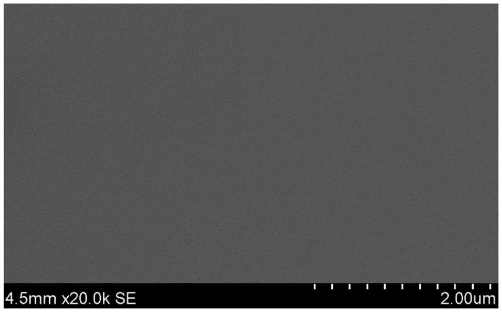
A method for preparing a self-supporting film for hydrogen-boron fusion target film
A self-supporting thin film and fusion target technology, which is applied in the direction of superimposed layer plating, vacuum evaporation plating, coating, etc., can solve the problems of insufficient self-supporting strength of ultra-thin boron film, easy cracks, and unsatisfactory, to achieve The adsorption position is evenly distributed, the strength is improved, and the surface is smooth
- Summary
- Abstract
- Description
- Claims
- Application Information
AI Technical Summary
Problems solved by technology
Method used
Image
Examples
preparation example Construction
[0053] In the above method for preparing a boron film, the thick film refers to a film with a thickness of 1000 nm to 10000 nm, and the thin film refers to a film with a thickness of 90 nm to 999 nm.
[0054] When the film-forming (boron film) method used in step (2) is different from the film-forming (film release agent) method used in step (1), the temperature of the silicon dioxide film needs to be lowered to After room temperature, start step (2).
[0055] When the film-forming (boron film) method used in step (2) is the same as the film-forming (release agent) method used in step (1) (for example, both are magnetron sputtering, or both are chemical vapor deposition methods), The same heating parameters are used, and the preparation of the boron film can be continued without cooling after the preparation of the release agent, which can reduce the stress of the film, improve the film quality of the target film, and shorten the preparation time of the target film. Therefore...
Embodiment 1
[0069] This embodiment is used to illustrate a method for preparing a silicon dioxide film on a substrate by thermal oxidation, and a method for preparing a micron-thick boron film by magnetron sputtering, which specifically includes the following steps:
[0070] (1) Using the silicon wafer as the substrate, first use deionized water, acetone and alcohol to clean in an ultrasonic cleaner for 20 minutes each, put it into a tube furnace immediately after drying, and preheat it at 1000 ° C for 1 hour to dry it. Pure oxygen is used as an oxidizing atmosphere to directly react with silicon to generate silicon dioxide at 1000 °C, and a silicon dioxide film with a thickness of 300 nm and a roughness of less than 1 nm is prepared.
[0071] (2) Preheating the cooled silicon wafer substrate with silicon dioxide film at 600°C for 1 hour, using the boron target as the boron source, argon as the sputtering gas, and the radio frequency power supply as the excitation source, at 0.4 Pa A 1.5-...
Embodiment 2
[0074] This embodiment is used to illustrate a method for preparing a silicon dioxide thin film on a substrate by a thermal oxidation method, and a method for preparing a nano-scale boron film by a magnetron sputtering method.
[0075] The difference between this embodiment and Embodiment 1 is that, in step (2), a boron film with a thickness of 90 nanometers is prepared on the silicon dioxide film under a pressure of 0.9 Pa, a power of 80 watts, and a temperature of 900°C.
PUM
| Property | Measurement | Unit |
|---|---|---|
| surface roughness | aaaaa | aaaaa |
| thickness | aaaaa | aaaaa |
| thickness | aaaaa | aaaaa |
Abstract
Description
Claims
Application Information
