Semiconductor laser and planar optical waveguide coupling structure, optical path system and manufacturing method

A planar optical waveguide and coupling structure technology, applied in the field of optical system and manufacturing, semiconductor laser and planar optical waveguide coupling structure, can solve the problem of effective refractive index mismatch of mode spot size, low coupling efficiency, etc., to achieve cost advantages, coupling Simple structure and small volume

Inactive Publication Date: 2021-06-04
QXP TECH INC
View PDF3 Cites 1 Cited by
  • Summary
  • Abstract
  • Description
  • Claims
  • Application Information

AI Technical Summary

Problems solved by technology

However, due to the mismatch of spot size and effective refractive index between the semiconductor laser and the planar optical waveguide multiplexing device, the coupling efficiency is not high

Method used


Image

  • Semiconductor laser and planar optical waveguide coupling structure, optical path system and manufacturing method
  • Semiconductor laser and planar optical waveguide coupling structure, optical path system and manufacturing method
  • Semiconductor laser and planar optical waveguide coupling structure, optical path system and manufacturing method

Examples


Embodiment Construction

[0033] The following will clearly and completely describe the technical solutions in the embodiments of the present invention with reference to the accompanying drawings in the embodiments of the present invention. Obviously, the described embodiments are only some, not all, embodiments of the present invention. Based on the embodiments of the present invention, all other embodiments obtained by persons of ordinary skill in the art without making creative efforts belong to the protection scope of the present invention.

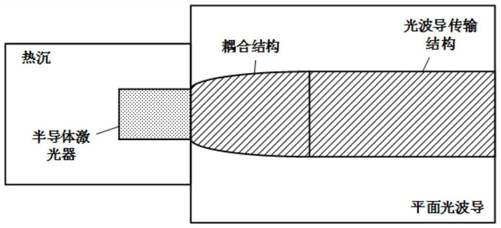
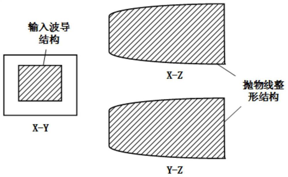
[0034] refer to figure 1 , figure 2 and image 3 , the present invention provides a semiconductor laser and a planar optical waveguide coupling structure, the coupling structure includes an input waveguide structure and a parabolic shaping structure, the input waveguide structure is located at one end of the parabolic shaping structure, and the waveguide structure of the parabolic shaping structure is parabolic, It is used to increase the mode matching with...


PUM


Abstract

The invention discloses a semiconductor laser and planar optical waveguide coupling structure, an optical path system and a manufacturing method, and relates to the technical field of semiconductor laser. The coupling structure comprises an input waveguide structure and a parabola shaping structure, the input waveguide structure is located at one end of the parabola shaping structure, and the waveguide structure of the parabola shaping structure is parabola-shaped; the input waveguide structure is tightly attached to the output end of the semiconductor laser, the size of the input waveguide structure is matched with the spot size of the semiconductor laser, and the end, away from the input waveguide structure, of the parabola shaping structure is connected with the optical waveguide transmission structure. The coupling structure provided by the invention is a structure in which the semiconductor laser and the planar optical waveguide are directly coupled, and compared with an optical path coupling structure of a laser-lens-planar optical waveguide device, the coupling structure has the advantages that elements such as a lens are reduced, the optical path structure is simple, the coupling efficiency is high, the assembly process is simple, and the cost is more advantageous; and the coupling structure is suitable for batch production.

Description

technical field [0001] The invention relates to the technical field of semiconductor lasers, in particular to a semiconductor laser and a planar optical waveguide coupling structure, an optical path system and a manufacturing method. Background technique [0002] With the rapid development of 5G optical communications and data centers, as well as the large demand for cloud computing, cloud storage and other services, the demand for high-speed optical modules in the market continues to grow. In order to expand bandwidth and increase network capacity, wavelength division multiplexing (WDM) technology has been widely used in optical modules. The optical transmission module based on WDM technology mainly includes: N-channel semiconductor lasers, N coupling lenses, planar optical waveguide multiplexing devices, isolators (1 or N), optical fiber connectors and output ports and other structures. Among them, the optical coupling between the semiconductor laser and the planar optica...

Claims


Application Information

Patent Timeline
Patent Type & Authority Applications(China)
IPC IPC(8): G02B6/42G02B6/122
CPCG02B6/4296G02B6/1228
Inventor 郭菲程东范修宏徐之光庄礼杰
Owner QXP TECH INC
Why Eureka
Try Eureka