Hybrid integrated optical communication waveband on-chip quantum entanglement source

A hybrid integration and quantum entanglement technology, applied in optics, nonlinear optics, instruments, etc., can solve problems such as reducing the brightness of entangled two-photons, the impact of entangled two-photon applications, and reducing the purity of entangled two-photons, achieving high integration and reducing Effects using space, high brightness

Active Publication Date: 2021-06-11
UNIV OF ELECTRONICS SCI & TECH OF CHINA
View PDF6 Cites 3 Cited by
  • Summary
  • Abstract
  • Description
  • Claims
  • Application Information

AI Technical Summary

Problems solved by technology

In order to improve the scalability of the quantum communication system, it is necessary to increase the integration of the quantum entanglement source. Since the second-order nonlinear waveguide has the characteristics of small size and easy integration, fiber coupling is usually used to make the pump light into the second-order nonlinear waveguide. The waveguide generates entangled two-photons in the optical communication band. However, the photons generated by the spontaneous Raman scattering process of the pump light in the fiber will enter the second-order nonlinear waveguide along with the pump light, and the remaining pump light will also follow the entangled double photons. Photons are output from the second-order nonlinear waveguide and enter the entangled two-photon transmission channel. Noise photons are generated through the spontaneous Raman scattering process in the transmission fiber, thereby reducing the purity of the entangled two-photon and seriously affecting the application of the entangled two-photon.
In order to reduce the number of noise photons, the power of the pump light can be reduced, but the brightness of the entangled two-photons is inevitably reduced

Method used


Image

  • Hybrid integrated optical communication waveband on-chip quantum entanglement source
  • Hybrid integrated optical communication waveband on-chip quantum entanglement source
  • Hybrid integrated optical communication waveband on-chip quantum entanglement source

Examples


Embodiment Construction

[0039] The principles and features of the present invention will be described below with reference to the accompanying drawings, and the exemplary examples are intended to be construed as they are intended to limit the scope of the invention.

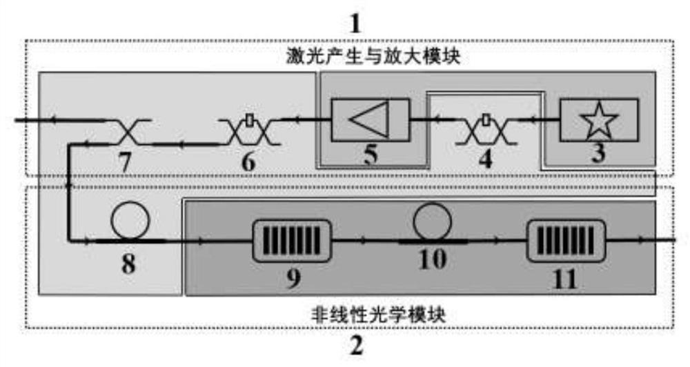
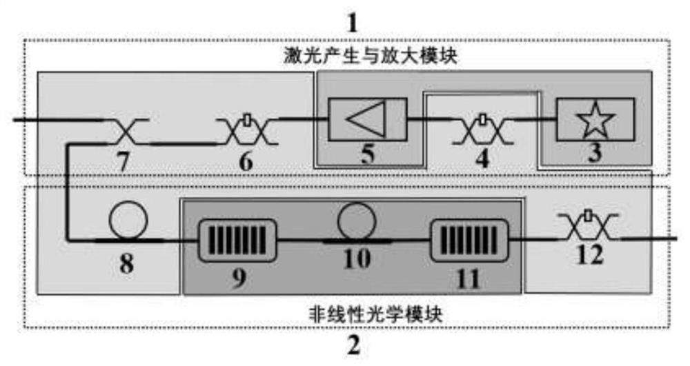
[0040] Such as figure 1 As shown, a quantum entanglement source provided by a mixed integrated optical communication band piece provided by the first embodiment of the present invention, including laser generation and amplifying module 1 and a non-linear optical module 2, the laser generating and amplifying module 1 and the non- Linear optical module 2 is integrated on the same substrate material;

[0041] The laser generating and the amplifying module 1 includes a continuous laser 3, an intensity modulator 4, a light amplifier 5, a tunable-optic atractor 6, and a beam splitter 7;

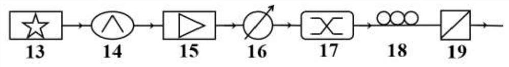
[0042] The DC pump light of the optical communication band generated by the continuous laser 3 produces a continuous pump Pu Lang or a double pulse pump, and th...


PUM


Abstract

The invention relates to a hybrid integrated optical communication waveband on-chip quantum entanglement source, which comprises a laser generation and amplification module and a nonlinear optical module, the nonlinear optical module is formed by connecting two sections of nonlinear waveguides through a second harmonic filter; under the action of optical communication waveband pump light, second harmonic generation and spontaneous parametric down-conversion processes successively occur in the two sections of nonlinear waveguides, so that quantum entanglement two-photon generation is realized. The second harmonic filter connected with the two waveguides can effectively restrain residual pump light, and noise is prevented from being introduced into entangled two photons in the spontaneous Raman scattering process. All devices required by the on-chip quantum entanglement source are integrated on the same substrate material, so that the volume of the quantum entanglement source is effectively reduced. The hybrid integrated optical communication waveband on-chip quantum entanglement source provided by the invention has the characteristics of high integration level, high brightness and low noise, can be realized through an advanced micro-nano processing and packaging technology, and is beneficial to the integration and practical development of quantum light sources.

Description

Technical field [0001] The present invention belongs to the field of quantum detection and quantum network technology, and more particularly to a mixed integrated optical communication band piece on quantum entanglement source. Background technique [0002] Optical communication band entangled dual-photons are the most important resources in the field of light quantum detection and light quantum network, which has a wide range of applications in fiber-based high-precision quantum detection and quantum networks: in quantum imaging, distributed quantum sensing, fiber quantum quantum An important role in stealth and other programs. The existing quantum entanglement sources built by the optical communication commercial device is complex and bulky, thereby reducing the scalability of quantum communication systems. Preparation of entangled double photons is generally based on spontaneous parameters in second-order or third-order nonlinear medium, with respect to the third-order nonline...

Claims


Application Information

Patent Timeline
Patent Type & Authority Applications(China)
IPC IPC(8): G02F1/39G02F1/365G02F1/35G02F1/355G02F1/00
CPCG02F1/39G02F1/365G02F1/353G02F1/355G02F1/0018
Inventor 周强张子昌袁晨智邓光伟宋海智王浟
Owner UNIV OF ELECTRONICS SCI & TECH OF CHINA
Why Eureka
Try Eureka