Deep trench MOSFET terminal structure and preparation method thereof
A terminal structure and deep groove technology, which is applied in semiconductor/solid-state device manufacturing, semiconductor devices, electrical components, etc., can solve the problems of limited device withstand voltage, high on-resistance, and reduced reliability, and achieve improved on-resistance , the injection concentration is small, and the effect of improving the withstand voltage characteristics
- Summary
- Abstract
- Description
- Claims
- Application Information
AI Technical Summary
Problems solved by technology
Method used
Image

Examples
Embodiment 1
[0089] see figure 1 , the present invention provides a method for preparing a deep trench MOSFET termination structure, the preparation method of the deep trench MOSFET termination structure comprising steps:
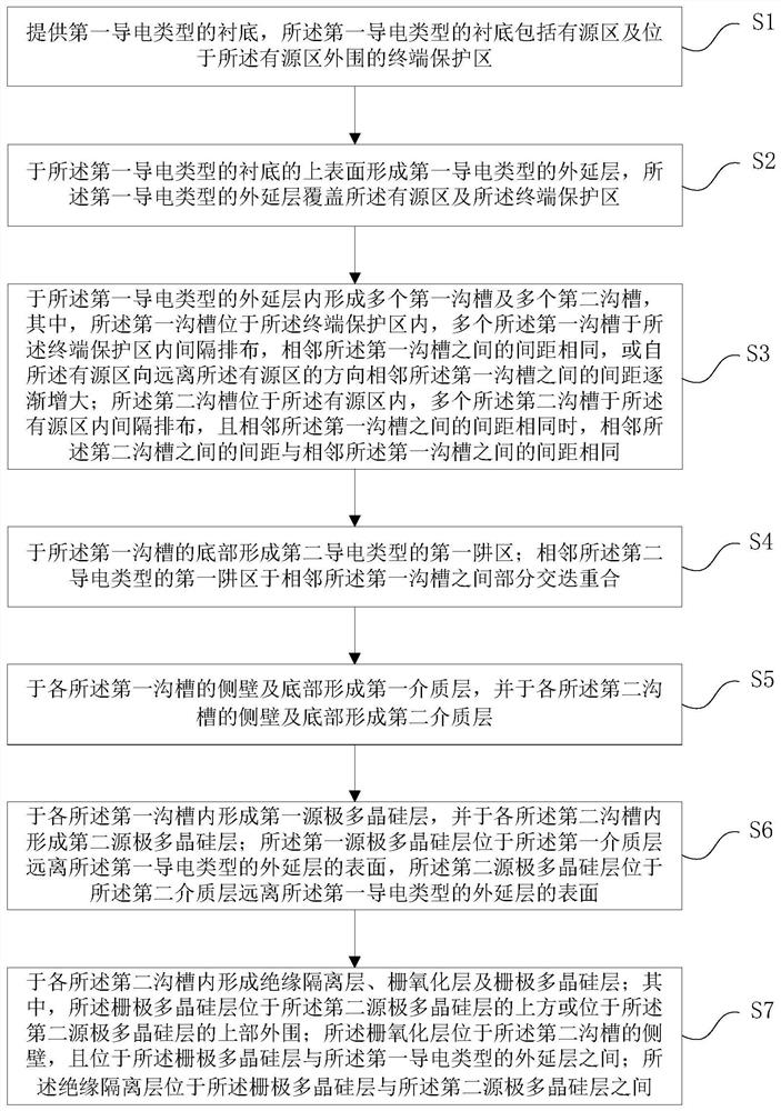
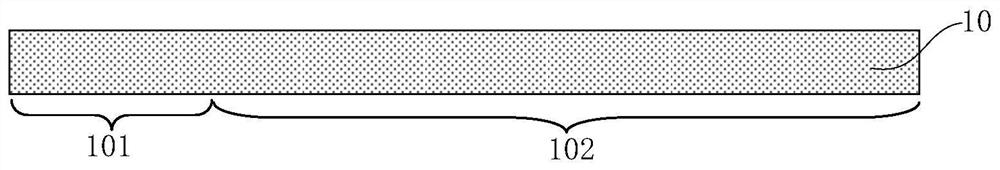
[0090] 1) providing a substrate of the first conductivity type, the substrate of the first conductivity type includes an active region and a terminal protection region located on the periphery of the active region;
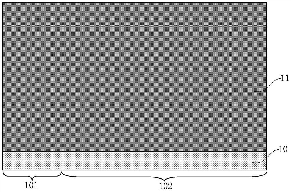
[0091] 2) forming an epitaxial layer of the first conductivity type on the upper surface of the substrate of the first conductivity type, the epitaxial layer of the first conductivity type covering the active region and the terminal protection region;
[0092] 3) forming a plurality of first trenches and a plurality of second trenches in the epitaxial layer of the first conductivity type, wherein the first trenches are located in the terminal protection area, and the plurality of first trenches Grooves are arranged at intervals in the terminal protection a...
Embodiment 2
[0152] Please combine Figure 2 to Figure 11 read on Figure 12 , the present invention also provides a deep trench MOSFET terminal structure, the deep trench MOSFET terminal structure includes: a substrate 10 of the first conductivity type, the substrate 10 of the first conductivity type includes an active region 101 and a The terminal protection area 102 on the periphery of the active area 101; the epitaxial layer 11 of the first conductivity type, the epitaxial layer 11 of the first conductivity type is located on the upper surface of the substrate 10 of the first conductivity type, and covers the The active area 101 and the terminal protection area 102; a plurality of first trenches 12, the first trenches 12 are located in the epitaxial layer 11 of the first conductivity type and are located in the terminal protection area 102 a plurality of the first grooves 12 are arranged at intervals in the terminal protection area 102; the distance between the adjacent first grooves ...
Embodiment 3
[0185] Please combine Figure 1 to Figure 12 refer to Figure 13 to Figure 17 , the present invention also provides a method for preparing a deep trench MOSFET terminal structure, the method for preparing a deep trench MOSFET terminal structure described in this embodiment is the same as the method for preparing a deep trench MOSFET terminal structure described in Example 1 roughly the same, the difference between the two lies in the difference between step 6) and step 7), specifically: the upper surface of the second dielectric layer 17 and the second source polysilicon obtained in step 6) in the first embodiment The upper surfaces of the layers 18 are lower than the upper surface of the epitaxial layer 11 of the first conductivity type, such as Figure 8 As shown, while the upper surface of the second dielectric layer 17 obtained in step 6) of this embodiment is lower than the upper surface of the epitaxial layer 11 of the first conductivity type, the second source polysili...
PUM
 Abstract
Description
Claims
Application Information
 - Generate Ideas
- Intellectual Property
- Life Sciences
- Materials
- Tech Scout
- Unparalleled Data Quality
- Higher Quality Content
- 60% Fewer Hallucinations
Browse by: Latest US Patents, China's latest patents, Technical Efficacy Thesaurus, Application Domain, Technology Topic, Popular Technical Reports.
© 2025 PatSnap. All rights reserved.Legal|Privacy policy|Modern Slavery Act Transparency Statement|Sitemap|About US| Contact US: help@patsnap.com