Broadband adjustable light and thin structure type ceramic-based wave-absorbing material and cross-scale design and preparation method thereof

A wave absorbing material and ceramic-based technology, applied in the field of wave absorbing materials, can solve the problems of limited improvement of material wave absorbing performance, poor electromagnetic designability, poor mechanical properties, etc., and achieve the effect of electromagnetic designability of flexible materials

Active Publication Date: 2021-06-15
NORTHWESTERN POLYTECHNICAL UNIV
View PDF3 Cites 9 Cited by
  • Summary
  • Abstract
  • Description
  • Claims
  • Application Information

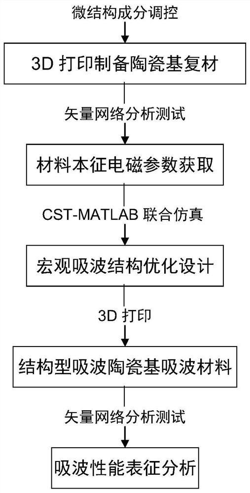
AI Technical Summary

Problems solved by technology

Solve the problems of poor electromagnetic designability and poor mechanical properties of existing wave-absorbing materials and the lim

Method used


Image

  • Broadband adjustable light and thin structure type ceramic-based wave-absorbing material and cross-scale design and preparation method thereof
  • Broadband adjustable light and thin structure type ceramic-based wave-absorbing material and cross-scale design and preparation method thereof
  • Broadband adjustable light and thin structure type ceramic-based wave-absorbing material and cross-scale design and preparation method thereof

Examples


Embodiment 1

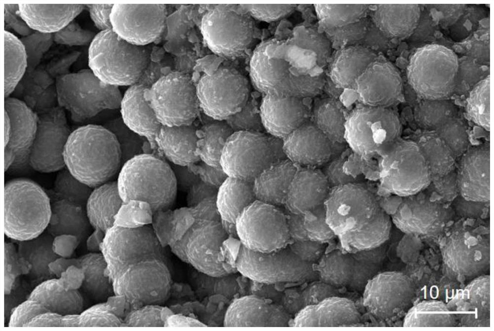
[0045] (1) Use Al 2 O 3 Photo curing ceramic slurry passes the single layer flat structure Al via the Form 2SLA photocurable 3D printer 2 O 3 Ceramic embryo, placed in the tube furnace in the air atmosphere of 5 ° C / min to 1500 ° C, after holding up for 6 hours, then cooled with the furnace to obtain a decentralized Al 2 O 3 ceramics.

[0046] (2) Using the CVI process in Al 2 O 3 SiC whiskers on the substrate (SiC w ), The growth temperature is 1000 ° C, the growth time is 150 hours, resulting in a flat plate structure Al 2 O 3 / SIC w Composite.

[0047] (3) Will the prepared Al 2 O 3 / SIC w The composite is cut and polished into an annular size of 3.01 mm, outer diameter of 7mm, thickness 3 mm. Using the vector network analysis tester to test the electromagnetic parameters of the radar full-band material, the parameter is substituted into the CST electromagnetic simulation software while using MATLAB pair Taxi-flat double-layer composite structure parameterization modeling, ...

Embodiment 2

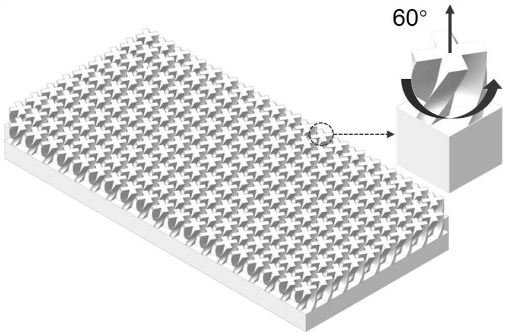
[0055] Preparation of 90 ° Trummer - Flat-plate composite structural Al in accordance with an example 2 O 3 / SIC w Ceramic base absorbing material verifies its microwave absorption performance.

[0056] by Figure 4 It can be seen, 90 ° cross twisted - flat-plate composite structural Al 2 O 3 / SIC w Ceramic base absorbing material Get RL at 10.9 GHz min = -47.4dB, the corresponding material thickness was 3.45 mm; the maximum EAB was 4.0 GHz, the corresponding thickness was 3.60 mm.

[0057] In summary, 90 ° cross twisted - flat-plate composite structural Al 2 O 3 / SIC w Ceramic base absorbing material relative to 60 ° torsion angle, its RL min And the corresponding frequency, the maximum EAB has changed significantly, indicating that the change of the ceramic base reciprocity can be achieved by the cross twisting angle change, indicating the cross twisted - flat-plate composite structural Al1 2 O 3 / SIC w The ceramic base absorbing material is a wide frequency adjustable thin s...

Embodiment 3

[0059] (1) Mix 15 wt% carbon nanotube (CNT) into a photocurable molded SiO 2 In the ceramic slurry, the magnetic stirrer is used for mechanical stirring for 5 hours, then ultrasonic emulsified dispersing machine is used to perform ultrasonic dispersion for 1 hour, thereby preparing a CNT dispersion uniform optical curing SiO. 2 / CNT ceramic slurry.

[0060] (2) Using Long Ceraform 100DLP Photocoction 3D Printed Panel Structure SIO 2 / CNT composite ceramic embryo. Thereafter, in the tubular furnace, in the nitrogen atmosphere, the temperature of the temperature of 5 ° C / min is 1000 ° C, and after 3 hours, the furnace is cooled to obtain a decentralized SiO. 2 / CNT composite.

[0061] (3) The SIO prepared 2 / CNT composites are cut and polished into an annular size of 3.01 mm, outer diameter of 7mm, and thickness 3 mm, and use the vector network analysis tester to obtain 2 to 18 GHz eccenter electromagnetic parameters, and substitute the parameter into the CST electromagnetic s...


PUM

PropertyMeasurementUnit
Densityaaaaaaaaaa
Diameteraaaaaaaaaa
Minimum reflection lossaaaaaaaaaa

Abstract

The invention relates to a broadband adjustable light and thin structure type ceramic-based wave-absorbing material and a cross-scale design and preparation method thereof. The electromagnetic performance of the wave-absorbing material is regulated and controlled by combining macro-structure optimization with micro-structure component regulation and control through cross-scale collaborative design. On the basis of an existing wave-absorbing material, a flexible 3D printing technology and microstructure component regulation and control processes such as chemical vapor impregnation (CVI) and polymer impregnation and pyrolysis (PIP) are utilized to realize organic combination of a ceramic wave-transparent phase and a wave-absorbing agent medium; and finally, the high-compression-ratio ceramic-based wave-absorbing material which has good impedance matching characteristics and high attenuation characteristics and is thin in thickness, light in weight, wide in frequency band and adjustable in frequency is prepared, a new thought is provided for design and preparation of the structure-function-integrated broadband-adjustable light and thin structural wave-absorbing material, and the urgent requirement of modern combat aircrafts for novel stealth materials is met.

Description

Technical field [0001] The present invention belongs to the technical field of absorbent material, and is related to a wide frequency adjustable thin structure type ceramic base absorbing material and a span scale design and preparation method. Background technique [0002] With the continuous advancement of radar detection technology, the stealth performance of the aircraft has become an important factor affecting its safety and reliability. Materials are stealth to improve the basic method of improving the stealth performance of the aircraft. The traditional absorbent coating is less than: one is a narrow, fixed, fixed, unable to cope with new broadband radar, while improving the absorbent content or increasing the thickness of the coating to broaden the absorption frequency band, high push ratio The aircraft is not advisable; the second is low intensity, poor adhesion, easy wear, etc., resulting in high maintenance costs. Ceramic base composites have important application pros...

Claims


Application Information

Patent Timeline
IPC IPC(8): C04B35/10C04B35/48C04B35/56C04B35/589C04B35/622C04B35/80B33Y10/00B33Y70/00
CPCC04B35/10C04B35/48C04B35/5603C04B35/589C04B35/80C04B35/622B33Y10/00B33Y70/00C04B2235/5276C04B2235/5288C04B2235/422
Inventor 梅辉姚礼赵星成来飞
Owner NORTHWESTERN POLYTECHNICAL UNIV
Why Eureka
Try Eureka