Check patentability & draft patents in minutes with Patsnap Eureka AI!

A Magnetic Random Access Memory Based on Group III-V Narrow Bandgap Semiconductors

A magnetic random access memory, narrow bandgap technology, applied in the field of electronics, can solve the problems of memory bank downtime reading, failure, affecting the operation efficiency of the memory bank, etc., to improve the operation effect, reduce the hidden danger of downtime, improve the timeliness and The effect of durability

Active Publication Date: 2022-03-11
HUNAN UNIV OF SCI & TECH
View PDF5 Cites 0 Cited by
  • Summary
  • Abstract
  • Description
  • Claims
  • Application Information

AI Technical Summary

Problems solved by technology

[0004] In view of the deficiencies in the prior art, the purpose of the present invention is to provide a magnetic random access memory based on III-V narrow bandgap semiconductors, to solve the problem of preparing single-chip integrated magnetic memory based on III-V narrow bandgap photovoltaic semiconductor compound chip boards. Random access memory has a good medium to transmit electrical signals in terms of magnetoresistance properties, but the superimposed semiconductor plates will generate static particles and absorb dust particles due to the magnetic button wires, thus affecting the operation efficiency of semiconductor memory bars using bipolar transistors , causing the memory module to continue to crash or fail to read, affecting the running cache band of the computer host and the problem of database conversion operations

Method used


Image

  • A Magnetic Random Access Memory Based on Group III-V Narrow Bandgap Semiconductors
  • A Magnetic Random Access Memory Based on Group III-V Narrow Bandgap Semiconductors
  • A Magnetic Random Access Memory Based on Group III-V Narrow Bandgap Semiconductors

Examples


Embodiment 1

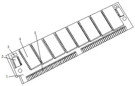
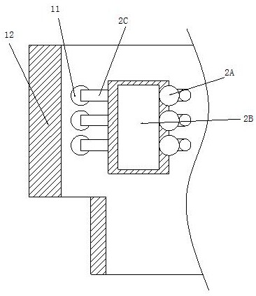
[0035] see Figure 1-Figure 8 , the present invention provides a kind of magnetic random access memory based on III-V group narrow-bandgap semiconductor, and its structure comprises: integrated circuit board 1, narrow-bandgap core frame board 2, resistance frame block 3, single-chip microcomputer board 4, copper sheet pin Plate 5, the narrow band gap core frame plate 2 is close to the lower left corner of the integrated circuit board 1 and is on the same vertical plane, the resistance frame block 3 is installed on the top of the narrow band gap core frame plate 2, so The single-chip microcomputer board 4 is provided with more than two and is all inserted and embedded in the front side of the integrated circuit board 1, and the copper sheet pin plate 5 is provided with more than two and is all closely attached to the bottom of the integrated circuit board 1. The narrow band gap core frame plate 2 is provided with an arc-extinguishing brush wheel rod 2A, a frequency conversion r...

Embodiment 2

[0043] see Figure 1-Figure 8 , the present invention provides a magnetic random access memory based on III-V narrow-bandgap semiconductors, other aspects are the same as in Embodiment 1, the difference is that:

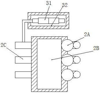
[0044] see image 3 , the resistance block 3 is composed of a resistance block 31 and a lead frame 32, the resistance block 31 is installed inside the lead frame 32, the resistance block 31 is electrically connected with the lead frame 32 and is on the same vertical plane On the other hand, through the resistance block 31 in the lead frame 32, a node is formed to increase the resistance value to regulate the operation effect of the steady flow.

[0045] see Image 6 , the resistance block 31 is made up of a resistance tube housing 311 and a copper core column block 312, the copper core column block 312 is installed inside the resistance tube housing 311, the resistance tube housing 311 and the copper core column block 312 Nested into one body and the axes are coll...


PUM


Abstract

The invention discloses a magnetic random access memory based on III-V narrow-bandgap semiconductors. Realized the use of the integrated circuit board and the narrow bandgap core frame board, through the built-in laminated composite circuit panel to guide the diode through-hole to connect the frequency conversion relay board and the narrow bandgap pin to form a cross-pass dislocation frequency conversion relay operation effect, Guarantee the increasing protection degree of the inclined frame bellows in the frequency conversion relay and the narrow band gap laminated relay operation effect of the semiconductor compound of the narrow band gap pin, and then improve the electromagnetic anti-interference strength of the magnetic random access memory and the separator through the arc-extinguishing brush wheel rod Electrostatic particles and dust particles improve the operation effect of the circuit panel with the refined structure of the central control input and output of the internal relay contact, improve the timeliness and durability of the memory, reduce the hidden danger of downtime, and improve the smooth storage operation efficiency.

Description

technical field [0001] The invention relates to a magnetic random access memory based on III-V group narrow bandgap semiconductors, which belongs to the field of electronics. Background technique [0002] The bipolar transistor storage and compound semiconductor storage of magnetic random access memory are highly efficient in operation, improve the storage density of the host computer and the high-speed computing efficiency of big data integration, and ensure the sensitivity and precision of continuous high-frequency data input and output reading of the memory stick. The current technology Common disadvantages to be optimized are: [0003] Based on the photovoltaic semiconductor compound chip board with narrow band gap of III-V family to prepare single-chip integrated magnetic random access memory, it has a good medium to transmit electric signals in the nature of magnetoresistance, but the superimposed semiconductor board will generate static electricity due to the magnetic...

Claims


Application Information

Patent Timeline
Patent Type & Authority Patents(China)
IPC IPC(8): H05K1/18G11C11/16
CPCH05K1/182G11C11/16
Inventor 胡仕刚高龙贡凯伦李炉焦
Owner HUNAN UNIV OF SCI & TECH
Features
  • R&D
  • Intellectual Property
  • Life Sciences
  • Materials
  • Tech Scout
  • Unparalleled Data Quality
  • Higher Quality Content
  • 60% Fewer Hallucinations
Learn More