Substrate leveling jig, leveling method and probe card

A substrate and fixture technology, applied in the field of probe cards, can solve the problems of overflowing tin and connecting tin, the pressure block cannot achieve uniform solder joints, and the flatness requirements cannot be met, so as to improve the flatness, avoid the decline of welding ability, The effect of improving test performance

Inactive Publication Date: 2021-07-02
上海泽丰半导体科技有限公司
View PDF12 Cites 0 Cited by
  • Summary
  • Abstract
  • Description
  • Claims
  • Application Information

AI Technical Summary

Problems solved by technology

However, due to the deformation of the required compact during reflow soldering, the force distributed by the compact on the substrate cannot reach the uniformity of each solder joint, resulting in solder jo

Method used


Image

  • Substrate leveling jig, leveling method and probe card
  • Substrate leveling jig, leveling method and probe card
  • Substrate leveling jig, leveling method and probe card

Examples


Embodiment Construction

[0050] In order to more clearly illustrate the technical solutions in the embodiments of the present invention or the prior art, the following will briefly introduce the drawings that need to be used in the description of the embodiments or the prior art. Obviously, the accompanying drawings in the following description are only These are some embodiments of the present invention. Those skilled in the art can also obtain other drawings based on these drawings without creative work.

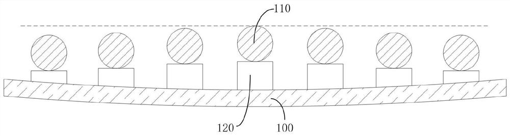
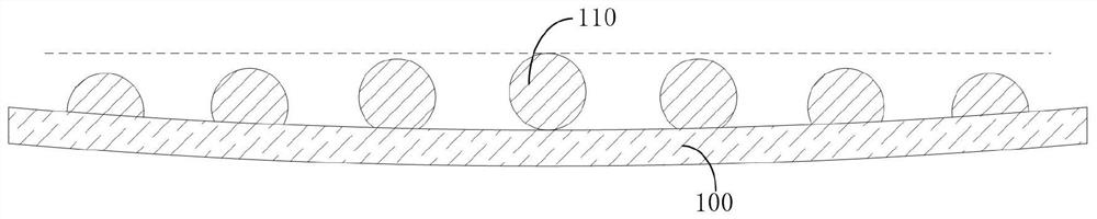
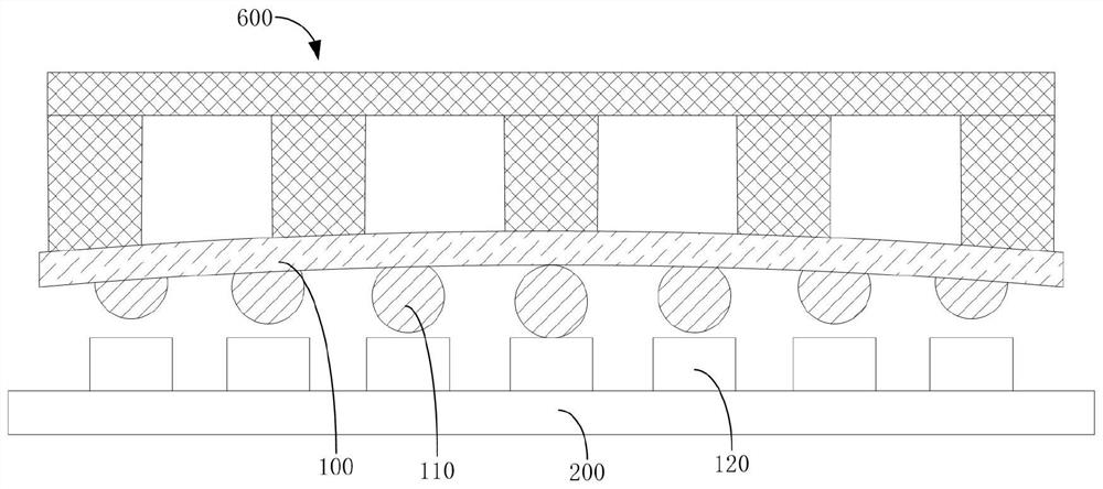
[0051] The space transformer can be a multi-layer organic board or a multi-layer ceramic board, which is used to fix metal probes for signal transmission with the chip and to test the parameters of the chip, hereinafter referred to as the substrate 100 . The precision of the vertical probe card in the horizontal and vertical directions largely determines the basic performance of the probe card in the test process. The precision may include the flatness of the test area of ​​the PCB test board 200 ...


PUM


Abstract

The invention discloses a substrate leveling jig, a leveling method and a probe card. The substrate leveling jig comprises a bearing platform, a locking device and a leveling device. The bearing platform is used for bearing a substrate. The locking device is used for locking the substrate on the bearing platform. A grinding mechanism of the leveling device is located above the substrate and is parallel to the bearing platform. Under the driving of a driving mechanism, the grinding mechanism is used for grinding welding spots on the upper surface of a solder ball, so that the multiple welding spots are located on a same plane. According to the substrate leveling jig, the leveling method and the probe card, the bearing platform enables the substrate to be in full contact with the grinding mechanism, ensures that the grinding mechanism can fully grind the welding spots on the upper surface of the solder ball, enables the multiple welding spots to be located on the same plane, and further can ensure that all the welding spots can be in full contact with the solder side of a PCB test board. The flatness of the substrate after being welded on the PCB test board can be improved to a great extent, so that the flatness error of the whole substrate is reduced to be within 50 mum, and the test performance of the manufactured probe card can be greatly improved.

Description

technical field [0001] The invention relates to the technical field of probe cards, in particular to a substrate leveling fixture, a leveling method and a probe card. Background technique [0002] In the field of semiconductors, the probe card is used to test and analyze the interface during the wafer manufacturing stage, and to test the chip parameters by connecting the test machine to transmit signals with the chip. The probe card directly contacts the probes with the pads on the chip to lead out the chip signal, and cooperates with peripheral testing equipment and software control to achieve the purpose of automatic measurement. Probe cards are widely used in wafer testing of technology products such as memory, logic, consumer, drive, and communication ICs, and are a very small part of the semiconductor industry. When the IC design is completed, an order will be placed to the foundry for production. After the wafer is fabricated but not cut and packaged, in order to ens...

Claims


Application Information

Patent Timeline
IPC IPC(8): B24B37/10B24B37/30B24B37/34B24B41/02B24B47/12B24B1/00G01R1/073
CPCB24B37/042B24B37/10B24B37/30B24B37/34B24B41/02B24B47/12B24B1/00G01R1/073
Inventor 张振明罗雄科陶克文
Owner 上海泽丰半导体科技有限公司
Why Eureka
Try Eureka