Graphene-assisted vanadium oxide thermo-optical modulator and preparation process thereof
A vanadium oxide thermo-optic and graphene technology, applied in the field of light modulation, can solve the problems of poor thermal stability of microring light modulators, large insertion loss of plasma light modulators, low extinction of electroabsorption light modulators, etc. The effect of wide wavelength range, low insertion loss and small size
- Summary
- Abstract
- Description
- Claims
- Application Information
AI Technical Summary
Problems solved by technology
Method used
Image
Examples
Embodiment approach 1
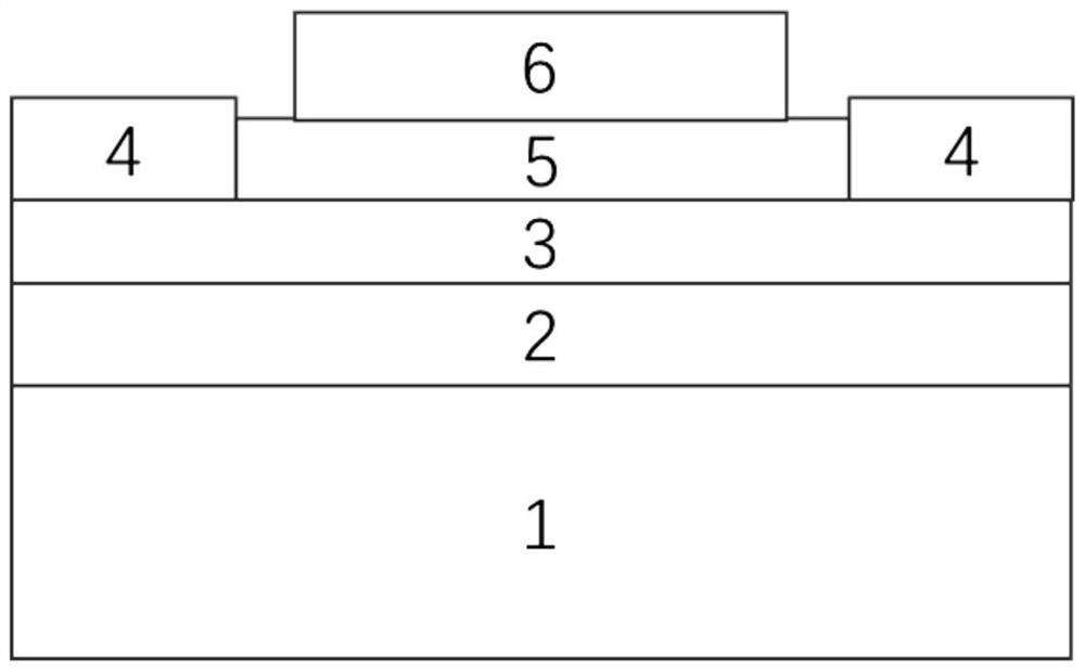
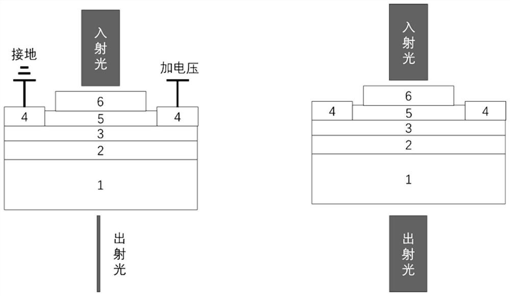
[0025] This embodiment provides a graphene-assisted vanadium oxide thermo-optic modulator, such as Figure 1-2 , comprising a substrate 1, a first insulating layer 2 formed on the substrate surface 1, a graphene layer 3 arranged on the first insulating layer 2, a second insulating layer 5 formed above the graphene layer 3, the The graphene-assisted vanadium oxide thermo-optic modulator also includes a metal electrode 4 deposited on the graphene layer 3 by photolithography or deposited on the second insulating layer by magnetron sputtering, reactive ion sputtering or deposited metal and then oxidized. 5 above the vanadium oxide film layer 6 .
[0026] The substrate is quartz, the first insulating layer is an ALD aluminum oxide layer with a thickness of 10-50nm, the second insulating layer is an ALD aluminum oxide layer with a thickness of 10-20nm, and the thickness of the vanadium oxide film layer is 50-200nm.
[0027] The metal electrode includes an adhesion layer in contact...
Embodiment approach 2
[0031] This embodiment provides a graphene-assisted vanadium oxide thermo-optic modulator, such as Figure 4 , comprising a substrate 1, a first insulating layer 2 formed on the surface of the substrate 1, a graphene layer 3 arranged on the first insulating layer 2, a second insulating layer 5 formed above the graphene layer 3, the graphite The ene-assisted vanadium oxide thermo-optic modulator also includes a metal electrode 4 deposited on the graphene layer 3 by photolithography or deposited on the second insulating layer 5 by magnetron sputtering, reactive ion sputtering or deposited metal and then oxidized. Vanadium oxide thin film layer 6 above.
[0032] The substrate is a silicon material, the first insulating layer is an ALD aluminum oxide layer with a thickness of 10-50nm, the second insulating layer is an ALD aluminum oxide layer with a thickness of 10-20nm, and the thickness of the vanadium oxide film layer is 50-200nm.
[0033] The metal electrode includes an adhe...
PUM
| Property | Measurement | Unit |
|---|---|---|
| thickness | aaaaa | aaaaa |
| thickness | aaaaa | aaaaa |
| thickness | aaaaa | aaaaa |
Abstract
Description
Claims
Application Information


