
On-chip integrated indirect band gap semiconductor white light source with high quantum luminous efficiency

A luminous efficiency, white light source technology, applied in optics, nonlinear optics, instruments, etc., can solve the problem of cost increase of new materials, and achieve the effect of improving luminous intensity and increasing luminous efficiency

Active Publication Date: 2021-07-02
SOUTH CHINA NORMAL UNIVERSITY
View PDF6 Cites 0 Cited by
  • Summary
  • Abstract
  • Description
  • Claims
  • Application Information

AI Technical Summary

Problems solved by technology

The cost of new materials will also increase significantly compared to the existing mature semiconductor industry

Method used


Image

  • On-chip integrated indirect band gap semiconductor white light source with high quantum luminous efficiency
  • On-chip integrated indirect band gap semiconductor white light source with high quantum luminous efficiency

Examples


Embodiment 1

[0041] The invention discloses a high-quantum luminous efficiency on-chip integrated indirect bandgap semiconductor white light source, which can inject high-concentration carriers into the semiconductor micro-nano structure through resonance, increase the temperature of the semiconductor micro-nano structure, and make the semiconductor reach the excitation condition of intrinsic energy, thereby Realize high-brightness white light emission, and provide a new micro-nano light source for on-chip integrated optical chips, all-silicon white light devices and related projects. Each will be described in detail below.

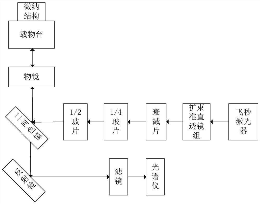
[0042] see figure 1 , the present invention provides a high quantum luminous efficiency on-chip integrated indirect bandgap semiconductor white light source, including femtosecond laser excitation optical path, semiconductor micro-nano structure and detection device, wherein:

[0043] The femtosecond laser excitation optical path includes a femtosecond laser, a beam ...

Embodiment 2

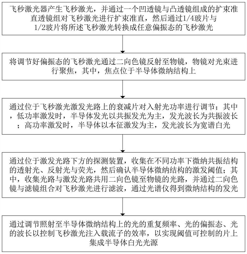
[0077] see figure 2 , the present invention also provides a method for improving the luminous quantum efficiency of an indirect bandgap semiconductor material, comprising the following steps:

[0078] S1. The femtosecond laser generates femtosecond laser, and converts the femtosecond laser into a femtosecond laser of any polarization state through 1 / 4 glass slide and 1 / 2 glass slide;

[0079] S2. Reflect the femtosecond laser with the adjusted polarization state to the objective lens through the dichroic mirror, and the objective lens focuses the beam, wherein the focus is located on the semiconductor micro-nano structure;

[0080] S3. Adjust the incident light power through the attenuation sheet located on the excitation optical path of the femtosecond laser; among them, when excited by low power, the semiconductor emits mainly by resonance, and the emission wavelength is the resonance wavelength; when excited by high power, the semiconductor emits by intrinsic Excitation-b...


PUM

PropertyMeasurementUnit
diameteraaaaaaaaaa
diameteraaaaaaaaaa

Abstract

The invention discloses an on-chip integrated indirect band gap semiconductor white light source with high quantum luminous efficiency. The on-chip integrated indirect band gap semiconductor white light source comprises: a femtosecond laser for generating femtosecond laser; a beam expanding and collimating lens group which is used for performing beam expanding and collimating on the femtosecond laser; an attenuation sheet which is used for adjusting the excitation power of the femtosecond laser; a polarization component which is used for controlling polarization of the femtosecond laser beam and can generate any adjustable polarization state; an objective lens which is used for receiving the excitation light beam and focusing the light beam on the semiconductor micro-nano structure; and a semiconductor micro-nano structure whcih is used for efficiently coupling exciting light, realizing resonance injection of carriers and increasing the temperature. The efficiency of injecting femtosecond laser into carriers is controlled by adjusting the repetition frequency, the polarization state and the wavelength of light irradiated to the semiconductor micro-nano structure, so that the threshold-controllable on-chip integrated semiconductor white light source is realized. The carrier injection efficiency of the micro-nano structure can be improved, and a brand new high-efficiency white light source is provided for an optical chip and a silicon optical device.

Description

technical field [0001] The invention relates to the technical field of semiconductor light sources, in particular to an on-chip integrated indirect bandgap semiconductor white light source with high quantum luminous efficiency. Background technique [0002] The photoluminescence spectrum of a semiconductor is closely related to its energy band structure characteristics. According to the definition of energy band structure, semiconductors can be divided into direct band gap semiconductors and indirect band gap semiconductors. Among them, because the Valence Band Maximum (VBM) of the direct bandgap semiconductor is in the same position as the Conduction Band Minimum (CBM) of the conduction band in the momentum space, its electrons are excited from the top of the valence band to the conduction band in the momentum space No phonon assistance is needed at the bottom. However, the electronic excitation process of indirect bandgap semiconductors requires the participation of phono...

Claims


Application Information

Patent Timeline
Patent Type & Authority Applications(China)
IPC IPC(8): G02F1/365G02F1/35
CPCG02F1/365G02F1/35G02F1/3501G02F1/3523G02F1/3526
Inventor 兰胜向进潘麦铭成
Owner SOUTH CHINA NORMAL UNIVERSITY
Features
  • Generate Ideas
  • Intellectual Property
  • Life Sciences
  • Materials
  • Tech Scout
  • Unparalleled Data Quality
  • Higher Quality Content
  • 60% Fewer Hallucinations
Learn More