Manufacturing method of separation gate power MOSFET device

A manufacturing method and separation gate technology, which are used in semiconductor/solid-state device manufacturing, semiconductor devices, electrical components, etc.

Active Publication Date: 2021-07-06
UNIV OF ELECTRONICS SCI & TECH OF CHINA
View PDF16 Cites 3 Cited by
  • Summary
  • Abstract
  • Description
  • Claims
  • Application Information

AI Technical Summary

Problems solved by technology

However, split-gate power MOSFET devices introduce parasitic capacitances associated with the split-gate electrode: the capacitance Cds between the drain and the split-gate electrode and the capacitance Cgs between the gate and the split-gate electrode, and the increased parasitic capacitance offsets to some extent The advantages of split-gate MOSFET devices to reduce gate-to-drain capacitance Cgd

Method used


Image

  • Manufacturing method of separation gate power MOSFET device
  • Manufacturing method of separation gate power MOSFET device
  • Manufacturing method of separation gate power MOSFET device

Examples


Embodiment 1

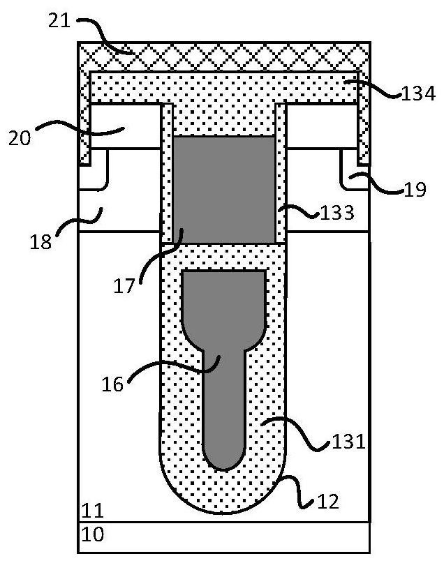
[0040] like image 3 As shown, a method for manufacturing a split gate power MOSFET device includes the following steps:

[0041] 1) A series of groove structures are formed on the epitaxial layer, and a first dielectric layer is formed on the inner wall of the groove structure;

[0042] 2) depositing polysilicon in the groove structure so that the polysilicon fills the entire groove;

[0043] 3) The polysilicon deposited in the etching step 2) forms the lower half of the stepped separation gate electrode in the control gate groove of the active region;

[0044] 4) wet etching the first dielectric layer, then depositing polysilicon in the groove structure, so that the polysilicon fills the entire groove;

[0045] 5) The polysilicon deposited in the etching step 4) forms the upper half of the stepped separation gate electrode in the control gate groove of the active region;

[0046] 6) depositing and etched back to form a second dielectric layer in the groove of the active reg...

Embodiment 2

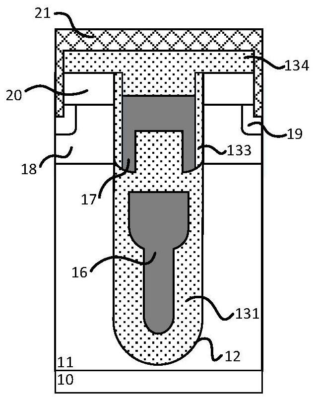
[0061] like Figure 4 As shown, this embodiment provides some steps of a method for manufacturing a split-gate power MOSFET device, which is used to replace image 3 In the (j)-(k) process, the difference between this embodiment and the manufacturing method described in Embodiment 1 is that step 9) can be implemented as follows:

[0062] 9) dry etching the oxide layer, controlling the etched interface to keep a certain distance from the upper interface of the stepped separation gate; then wet etching away the remaining silicon nitride in the groove;

Embodiment 3

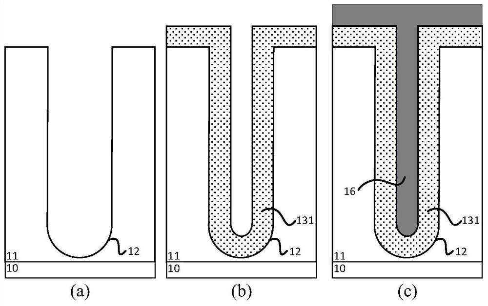
[0064] like Figure 5 As shown, the difference between this embodiment and the manufacturing method described in Embodiment 1 is that the first dielectric layer formed in step 1) surrounding the separated gate electrode adopts a low-k material with k less than 3.9 instead of silicon dioxide, which can further reduce the source-drain capacitance.


PUM


Abstract

The invention provides a manufacturing method of a separation gate power MOSFET device, which comprises the following steps of: after a dielectric layer between a control gate and a separation gate is formed, depositing or thermally growing a sacrificial oxide layer, depositing silicon nitride to fill the whole groove structure, and separating the silicon nitride from a silicon layer in an MESA region through the sacrificial oxide layer; after etching the silicon nitride, taking the silicon nitride reserved in the groove as a shielding layer for etching the oxide layer; etching the oxide layer until the interface of the oxide layer is higher than the upper interface of the stepped separation gate, and then etching the residual silicon nitride; and depositing polycrystalline silicon and performing back etching to form a control gate electrode. According to the device structure prepared by the invention, the lower half part of the control gate is relatively narrow, so that the gate-source capacitance Cgs can be greatly reduced, and meanwhile, the upper half part of the control gate increases the cross sectional area of gate current flowing, so that the gate resistance is reduced and the targets of high switching speed and low switching loss are achieved on the premise of ensuring that the gate-source capacitance Cgs and gate charge Qg are not degraded.

Description

technical field [0001] The invention belongs to the technical field of semiconductors, and more particularly, relates to a manufacturing method of a split gate power MOSFET device. Background technique [0002] With the continuous development of new fields in the electronic information industry, power semiconductor devices have also ushered in a new round of development peaks. At the same time, higher requirements have been placed on the performance of power MOSFETs. Lower switching losses and higher working efficiency have become the key points of power devices. development trend. The advantages of power VDMOS with high frequency and low power consumption are gradually manifested, especially in power management and other fields. The split gate power MOSFET device structure developed based on the Trench MOSFET device utilizes the split gate electrode to shield the capacitive coupling between the control gate electrode and the epitaxial layer to reduce the gate-drain parasit...

Claims


Application Information

Patent Timeline
Patent Type & Authority Applications(China)
IPC IPC(8): H01L21/336H01L21/283
CPCH01L29/66484H01L21/283H01L29/7813H01L29/407H01L29/42376H01L29/41766H01L29/66734Y02B70/10H01L29/41
Inventor 乔明马涛王正康张波
Owner UNIV OF ELECTRONICS SCI & TECH OF CHINA
Why Eureka
Try Eureka