

Semiconductor device and preparation method thereof
A semiconductor and device technology, applied in the field of semiconductor devices and their preparation, can solve the problems of easy lodging, decreased device performance and stability, large virtual line height and width, etc., to prevent lodging, improve performance and stability, and enhance strength. Effect
- Summary
- Abstract
- Description
- Claims
- Application Information
AI Technical Summary
Problems solved by technology
Method used
Image

Examples
Embodiment 1
[0049] Figure 2k The top view of the semiconductor device provided for this embodiment, Figure 2j for Figure 2kSectional view along the aa direction and bb direction. The semiconductor device is, for example, a memory device such as a Dynamic Random Access Memory (DRAM) element, but not limited thereto.
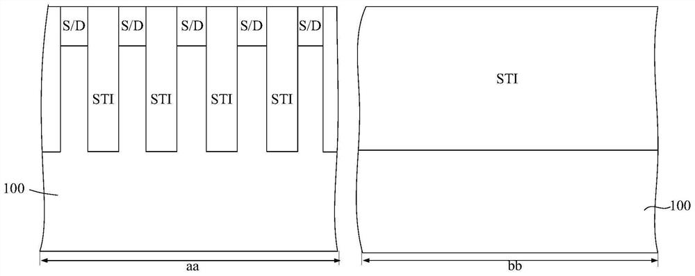
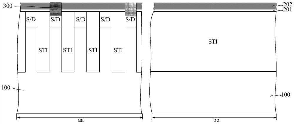
[0050] like Figure 2k and Figure 2j As shown, the semiconductor device includes a substrate 100 , a plurality of word lines WL formed in the substrate 100 , and a plurality of bit lines BL and a plurality of dummy lines DL formed on the substrate 100 .
[0051] The substrate 100 is, for example, a silicon substrate, a silicon containing substrate, an epitaxial silicon substrate, a silicon-on-insulator substrate, and the like.
[0052] Wherein, the substrate 100 defines a memory cell region 100A (memory cell region), a peripheral circuit region (periphery region, not shown), and a boundary region 100C between the memory cell region 100A and the peripheral circuit reg...
Embodiment 2
[0109] image 3 The cross-sectional views of the semiconductor device provided in this embodiment along the directions aa and bb. like image 3 As shown, the difference from Embodiment 1 is that in this embodiment, the virtual line DL further includes a third insulating layer 208a, and the third insulating layer 208a is located between the first insulating layer 206a and the second insulating layer 206a. between layers 207a.
[0110] In this embodiment, the first insulating layer 206a, the second insulating layer 207a and the third insulating layer 208a all contain at least two or more insulating materials, for example, the first insulating layer 206a, the second insulating layer 207a and the third insulating layer 208a are composed of two or more materials among silicon oxide, silicon nitride, and silicon oxynitride, and the materials of the first insulating layer 206a and the third insulating layer 208a can be the same Or different, preferably, the material of the first ins...
Embodiment 3
[0116] Figure 5 The cross-sectional views of the semiconductor device provided in this embodiment along the directions aa and bb. like Figure 5 As shown, the difference from Embodiment 1 and Embodiment 2 is that in this embodiment, part of the thickness of the bottom of the first insulating layer 206a of the virtual line DL extends laterally to the first insulating layer of the adjacent virtual line DL. The bottom of the layer 206a is connected to cover part of the surface of the substrate 100 in the interface region 100C.
[0117] read on Figure 5 , in this embodiment, all the first insulating layers 206a of the virtual lines DL extend laterally to form a single film layer, so that at least part of the surface of the substrate 100 in the boundary region 100C is also covered by the The first insulating layer 206a is covered.
[0118] When the semiconductor device in this embodiment is prepared, it is similar to Embodiment 1. First, according to Figure 2a ~ Figure 2h s...
PUM
 Abstract
Description
Claims
Application Information