Preparation method and application of NPB-like hole transport functional material
A technology of hole transport and functional materials, applied in the field of preparation of hole transport functional materials, can solve the problems of thickness and uniformity of photoconductor drum performance, low practical value, complex process, etc. The effect of simple structure and simple process
- Summary
- Abstract
- Description
- Claims
- Application Information
AI Technical Summary
Problems solved by technology
Method used
Image
Examples
Embodiment 1
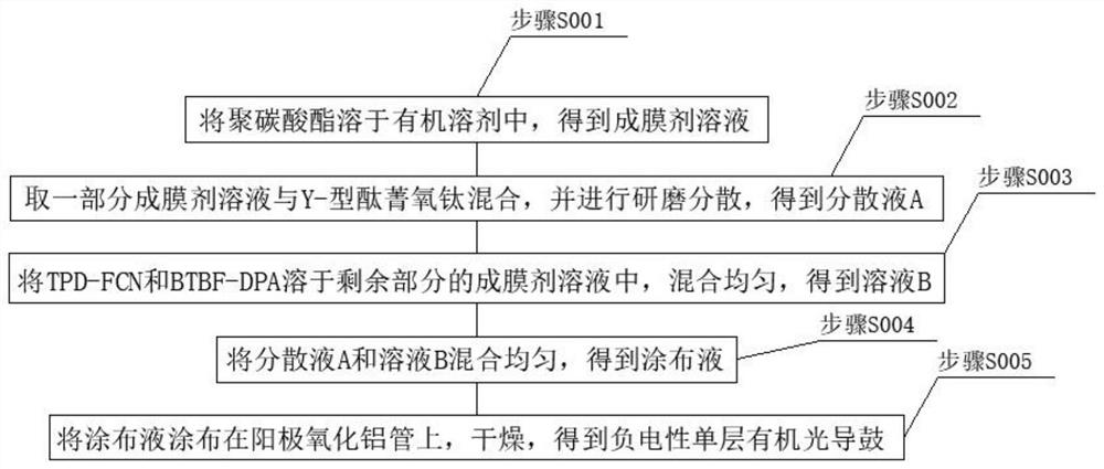
[0034] Polycarbonate (PCZ-300) is dissolved in THF to form a film-forming agent solution with a mass concentration of 10%; get 500 grams of 10% PCZ-300 solution, add 5 grams of Y-type titanium phthalocyanine, and disperse evenly with a ball mill. Then add 30 grams of m-TPD and 10 grams of N,N'-[4-(trifluoromethoxy)phenyl]-pyromellitic acid diamine, fully stir and dissolve to form a coating solution; adopt dip coating method, Apply the coating solution on the surface of the aluminum base of φ24*L250mm, and dry it for 2 hours to obtain a single-layer organic photosensitive drum with a photosensitive layer thickness of 15 μm.
Embodiment 2
[0036] Polycarbonate (PCZ-300) is dissolved in THF to form a film-forming agent solution with a mass concentration of 10%; get 500 grams of 10% PCZ-300 solution, add 5 grams of Y-type titanium phthalocyanine, and disperse evenly with a ball mill. Then add 30 grams of m-TPD and 10 grams of N,N'-[4-(trifluoromethylthio)phenyl]-pyromellitic acid diamine, fully stir and dissolve to form a coating solution; adopt dip coating method, Apply the coating solution on the surface of the aluminum base of φ24*L250mm, and dry it for 2 hours to obtain a single-layer organic photosensitive drum with a photosensitive layer thickness of 15 μm.
Embodiment 3
[0038] Except that no electron transport material is used, all other steps are the same as in Example 1.
[0039] Table 1 is the photoelectric performance parameter table of the organic photosensitive drum device involved in the present invention:
[0040]
[0041]
PUM
| Property | Measurement | Unit |
|---|---|---|
| particle diameter | aaaaa | aaaaa |
| thickness | aaaaa | aaaaa |
Abstract
Description
Claims
Application Information
 - R&D
- Intellectual Property
- Life Sciences
- Materials
- Tech Scout
- Unparalleled Data Quality
- Higher Quality Content
- 60% Fewer Hallucinations
Browse by: Latest US Patents, China's latest patents, Technical Efficacy Thesaurus, Application Domain, Technology Topic, Popular Technical Reports.
© 2025 PatSnap. All rights reserved.Legal|Privacy policy|Modern Slavery Act Transparency Statement|Sitemap|About US| Contact US: help@patsnap.com


