Flexible electrochromic device and preparation method thereof
An electrochromic layer and electrochromic technology, which is applied in the fields of instruments, nonlinear optics, optics, etc., can solve the problems of affecting the life of the functional layer of electrochromic devices, affecting the life of electrochromic devices, application and promotion limitations, etc. , to achieve the effect of prolonging the actual service life, widening the requirements of the preparation environment and reducing the production cost
- Summary
- Abstract
- Description
- Claims
- Application Information
AI Technical Summary
Problems solved by technology
Method used
Image
Examples
Embodiment 1
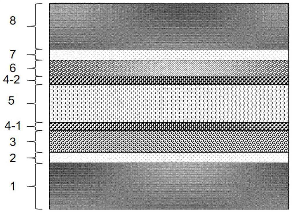
[0081] 1. The structure of the flexible electrochromic device: refer to the attached figure 1 , including: a first flexible substrate 1, a first conductive layer 2, an electrochromic layer 3, a first buffer medium layer 4-1, a quasi-solid electrolyte layer 5, and a second buffer medium layer 4-2, which are sequentially stacked. , an ion storage layer 6 , a second conductive layer 7 and a second flexible substrate 8 .
[0082] The materials of the first flexible substrate and the second flexible substrate are independently polyethylene terephthalate (PET), with a thickness of 125 μm and a transmittance of 91%.
[0083] Both the first conductive layer and the second conductive layer are tin-doped indium oxide (ITO) prepared by magnetron sputtering, and the resistance is 40Ω / □.
[0084] The electrochromic layer is tungsten oxide (WO) prepared by electron beam evaporation method. 3 ), with a thickness of 450nm.
[0085] Both the first buffer medium layer and the second buffer m...
Embodiment 2
[0097] 1. The structure of the flexible electrochromic device: refer to the attached figure 1 , including: a first flexible substrate 1, a first conductive layer 2, an electrochromic layer 3, a first buffer medium layer 4-1, a quasi-solid electrolyte layer 5, and a second buffer medium layer 4-2, which are sequentially stacked. , an ion storage layer 6 , a second conductive layer 7 and a second flexible substrate 8 .
[0098] Both the first flexible substrate and the second flexible substrate are polyimide (PI) films with a thickness of 100 μm and a transmittance of 89%.
[0099] Both the first conductive layer and the second conductive layer are tin-doped indium oxide (ITO) prepared by magnetron sputtering, and the resistance is less than 35 / □.
[0100] The electrochromic layer is titanium dioxide (TiO 2 ), with a thickness of 500nm.
[0101] The material of the first buffer dielectric layer is zirconia (ZrO 2 ), prepared by electron beam evaporation, with a thickness of ...
Embodiment 3
[0113] 1. The structure and composition of the flexible electrochromic device: including the first flexible substrate, the first conductive layer, the electrochromic layer, the first buffer medium layer, the quasi-solid electrolyte layer, the ion storage layer, the second a conductive layer and a second flexible substrate.
[0114] Both the first flexible substrate and the second flexible substrate are polyethylene naphthalate (PEN), with a thickness of 150 μm and a transmittance of 90%.
[0115] Both the first conductive layer and the second conductive layer are fluorine-doped tin oxide (FTO) prepared by magnetron sputtering, and the resistance is 50Ω / □.
[0116] The electrochromic layer is tungsten oxide (WO) prepared by magnetron sputtering. 3 ), with a thickness of 500nm.
[0117] The material of the first buffer dielectric layer is tantalum pentoxide (Ta 2 o 5 ), prepared by magnetron reactive sputtering method, the thickness is 150nm, the coating speed should be 0.4n...
PUM
| Property | Measurement | Unit |
|---|---|---|
| thickness | aaaaa | aaaaa |
| thickness | aaaaa | aaaaa |
| thickness | aaaaa | aaaaa |
Abstract
Description
Claims
Application Information


