
Ultraviolet light-emitting diode with p-i-n type multi-quantum well structure

A multi-quantum well structure, p-i-n technology, applied in the direction of electrical components, circuits, semiconductor devices, etc., can solve the problem of affecting the quantum efficiency or luminous efficiency of UV-LED devices, the reduction of electron and hole radiation recombination probability, and the suppression of UV-LED Light output capability and other issues

Active Publication Date: 2021-08-13
SOUTHEAST UNIV
View PDF4 Cites 2 Cited by
  • Summary
  • Abstract
  • Description
  • Claims
  • Application Information

AI Technical Summary

Problems solved by technology

The polarized electric field will cause the conduction band and valence band edge of the quantum well in the UV-LED to be tilted, so that the wave functions of electrons and holes are separated in space, resulting in a reduction in the probability of radiative recombination of electrons and holes, seriously Affect the internal quantum efficiency or luminous efficiency of UV-LED devices
[0003] In addition, when the Al composition of the p-type AlGaN layer of AlGaN-based UV-LEDs increases, the activation efficiency of p-type impurities (such as Mg) becomes low, which reduces the number of holes injected into the active region, and finally inhibits the UV- LED Light Output Capability

Method used


Image

  • Ultraviolet light-emitting diode with p-i-n type multi-quantum well structure
  • Ultraviolet light-emitting diode with p-i-n type multi-quantum well structure
  • Ultraviolet light-emitting diode with p-i-n type multi-quantum well structure

Examples


Embodiment Construction

[0018] The present invention will be further explained below in conjunction with the accompanying drawings.

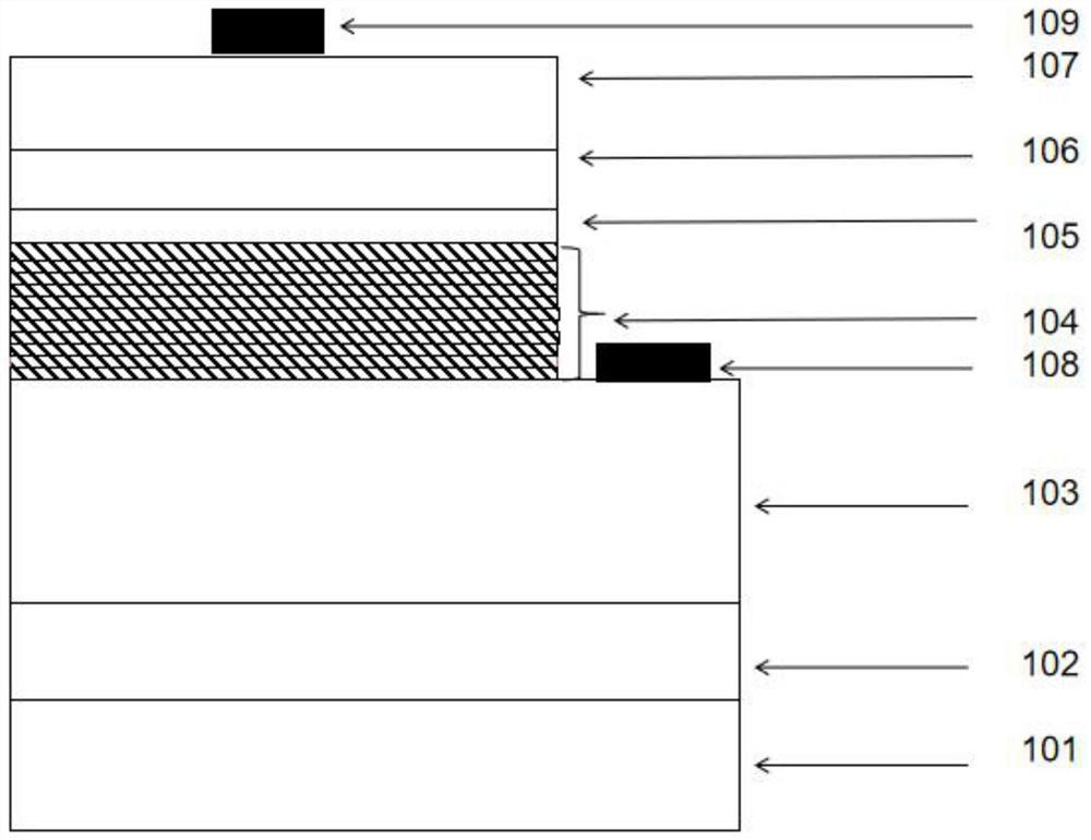
[0019] Such as figure 1 As shown, a UV-LED with a p-i-n type multi-quantum well structure of the present invention, a substrate 101, an AlN buffer layer 102, an n-type AlGaN layer 103, and a p-i-n type multi-quantum well active region 104 are sequentially arranged from bottom to top , an electron blocking layer 105, a p-type AlGaN layer 106, a p-type GaN ohmic contact layer 107, and an n-type electrode 108 arranged on the n-type AlGaN layer 103 and a p-type electrode 109 arranged on the p-type GaN ohmic contact layer 106 .

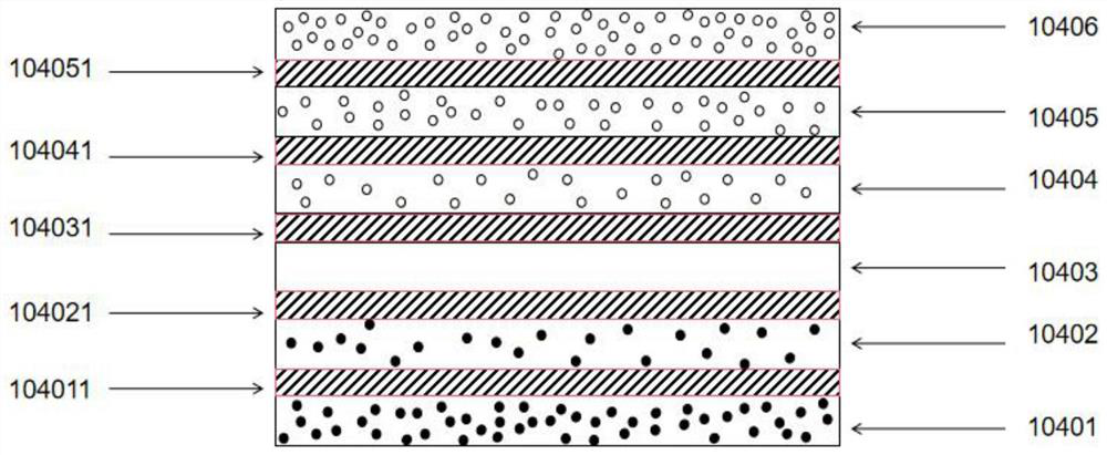
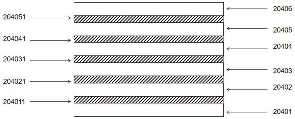
[0020] The quantum barriers in the p-i-n type multi-quantum well active region 104 are, from bottom to top, n-type doped quantum barriers with different doping concentrations, undoped i-type quantum barriers, and p-type doped quantum barriers with different doping concentrations. Quantum barriers, that is, from bottom to top quantum barriers are...


PUM

PropertyMeasurementUnit
Thicknessaaaaaaaaaa
Thicknessaaaaaaaaaa
Electron concentrationaaaaaaaaaa

Abstract

The invention discloses an ultraviolet light-emitting diode with a p-i-n type multi-quantum well structure. The ultraviolet light-emitting diode is provided with a substrate, an AlN buffer layer, an n-type AlGaN layer, a p-i-n type multi-quantum well active region, an electron blocking layer, a p-type AlGaN layer, a p-type GaN ohmic contact layer, an n-type electrode which is arranged on the n-type AlGaN layer and a p-type electrode which is arranged on the p-type GaN ohmic contact layer distributed from bottom to top in sequence. According to the ultraviolet light-emitting diode with the p-i-n type multi-quantum well structure, the carrier concentration and injection efficiency can be improved; an electric field opposite to an original built-in electric field in direction can be formed by utilizing the concentration difference of carriers in adjacent regions with different doping concentrations, and the original built-in electric field between a p type region and an n type region can be weakened, and the quantum limited stark effect caused by the built-in polarized electric field is reduced,so that the radiation recombination efficiency of electrons and holes is improved, and the light emitting power of the ultraviolet light-emitting diode is enhanced.

Description

technical field [0001] The invention relates to the manufacturing field of semiconductor optoelectronic materials and devices, in particular to an ultraviolet light emitting diode with a p-i-n type multi-quantum well structure. Background technique [0002] AlGaN-based ultraviolet light-emitting diodes (UV-LEDs) have the advantages of low energy consumption, environmental friendliness, and adjustable emission wavelengths, and can be widely used in printing ink curing, high-density data information storage, sterilization, healthcare, water and air purification and other fields. Due to the lack of GaN or AlN homogeneous substrates, AlGaN-based UV-LEDs usually use heterogeneous substrates, such as sapphire, silicon carbide, silicon and other substrates for growth. However, due to the large lattice mismatch between the heterogeneous substrate and the polar c-plane sapphire and other heterogeneous substrates, there are strong spontaneous polarization and piezoelectric The polar...

Claims


Application Information

Patent Timeline
IPC IPC(8): H01L33/00H01L33/06H01L33/32
CPCH01L33/0012H01L33/06H01L33/32
Inventor 张雄房瑞庭胡国华崔一平
Owner SOUTHEAST UNIV
Learn More