Silicon-carbon negative electrode material and preparation method thereof
A negative electrode material, silicon carbon technology, applied in the field of silicon carbon negative electrode materials and its preparation, can solve the problems of uneven dispersion of silicon nanoparticles, poor conductivity, and inability to be industrialized
- Summary
- Abstract
- Description
- Claims
- Application Information
AI Technical Summary
Problems solved by technology
Method used
Image
Examples
Embodiment 1
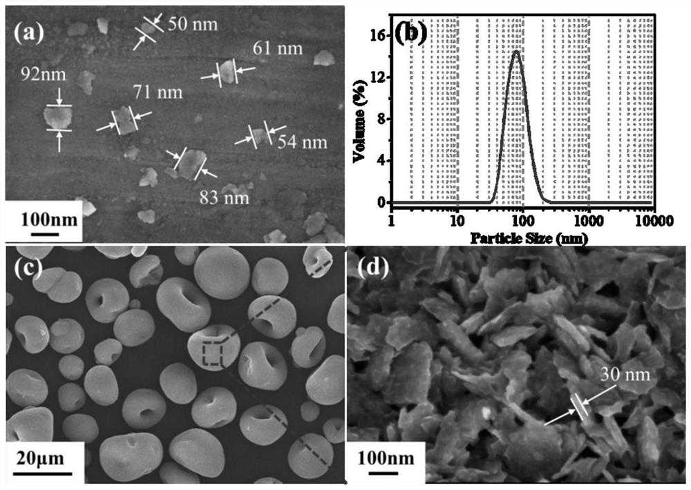
[0060]The micro-nano silicon powder used is prepared by the following method: the crystalline silicon bulk material is processed by electric spark discharge, the pulse width of the discharge pulse is 120μs, the duty ratio is 1:5, the open circuit voltage is 180V, and the local high temperature gasification is used. Deionized water is used as the working fluid, and after cooling, micro-nano silicon particles formed by the aggregation of silicon atom clusters are obtained; then mechanical grinding is carried out, using zirconia grinding balls with a diameter of 0.1mm, and the edge speed is 14.5m / s. The solvent is ethanol (with 1 wt% sodium hexametaphosphate added as a dispersant), and the ball milling time is 5 hours. The average particle size of the nano silicon particles is 10-100nm; the degree of amorphization is 90-99%; the average grain size is 1-15nm.
[0061] The preparation process of silicon carbon composite materials:
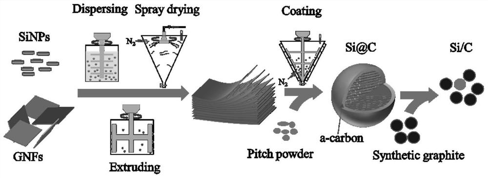
[0062] Step 1, weigh 1kg of nano-silicon powder,...
Embodiment 2
[0068] The difference from Example 1 is that in the first step, carbon nanotubes are also added. The ratio of nano silicon powder, graphite nano sheet, carbon nanotube and ethanol is 1:0.9:0.1:18.
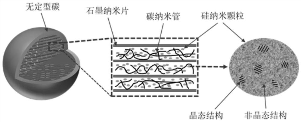
[0069] The silicon-carbon composite material uses 2-dimensional graphite nanosheets as the frame to form a conductive network with 1-dimensional carbon nanotubes. The 0-dimensional silicon nanoparticles are evenly dispersed in the conductive network and closely contacted. This 0-dimensional, 1-dimensional, The 2-dimensional composite structure greatly improves the conductivity of the particles and also increases the strength of the particles.
PUM
| Property | Measurement | Unit |
|---|---|---|
| particle size | aaaaa | aaaaa |
| thickness | aaaaa | aaaaa |
| specific surface area | aaaaa | aaaaa |
Abstract
Description
Claims
Application Information


