Multi-junction distributed feedback semiconductor laser and preparation method thereof

A distributed feedback, semiconductor technology, applied in semiconductor lasers, lasers, laser parts and other directions, can solve the problems of poor waveguide cross-section symmetry, large parasitic capacitance of devices, affecting fiber coupling, etc., to improve fiber coupling efficiency and reduce parasitic capacitance parameters. , the effect of high fiber coupling efficiency

Pending Publication Date: 2021-09-21
TSINGHUA UNIV
View PDF0 Cites 4 Cited by
  • Summary
  • Abstract
  • Description
  • Claims
  • Application Information

AI Technical Summary

Problems solved by technology

[0004] However, it is difficult for traditional DFB lasers to achieve high output optical power of 100mW and above. One of the important reasons is that traditional DFB lasers generally use a single PN junction to emit light, and the lateral optical field distribution of the output cavity surface is limited. The average optical power density is too large, which limits the further increase of laser power
In addition, since the luminous size in the epitaxial growth direction of the laser is smaller than the horizontal direction, the vertical divergence angle of the laser far field is much larger than the horizontal divergence angle, and finally an elliptical laser spot is output, resulting in poor symmetry of the transverse light field distribution in the waveguide section, which affects fiber coupling.
However, high-power laser output requires an increase in the size of the epitaxial growth direction. A thicker waveguide layer will introduce high-order transverse mode lasing, thereby increasing the far-field divergence angle of the laser, which is not conducive to improving the beam quality.
In addition, in order to achieve high power output, semiconductor lasers usually use a cavity length of more than mm order, and the parasitic capacitance of the device is large, which is not conducive to high-speed modulation of the laser

Method used


Image

  • Multi-junction distributed feedback semiconductor laser and preparation method thereof
  • Multi-junction distributed feedback semiconductor laser and preparation method thereof
  • Multi-junction distributed feedback semiconductor laser and preparation method thereof

Examples


specific preparation Embodiment 1

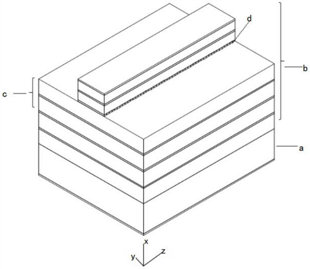
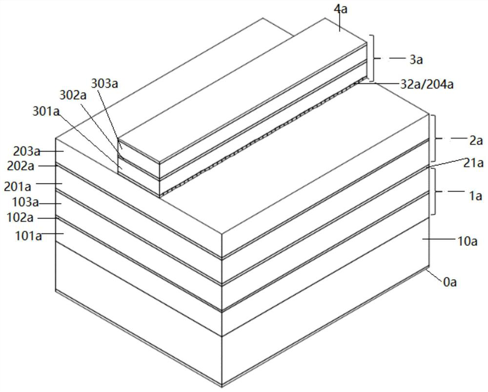
[0047] This specific embodiment introduces a preparation method of an InGaAsP / InP multi-junction distributed feedback semiconductor laser (DFB-LD) with a wavelength of 1550nm, as follows:

[0048] refer to figure 2 As shown, the following materials are epitaxially grown from bottom to top on a highly doped n-type InP substrate 10a: the first PN junction N region 101a is an n-type InP buffer layer (thickness 500nm, doping concentration about 1× 10 18 cm -3 ); the light-emitting region 102a of the first PN junction, wherein the light-emitting region 102a includes from bottom to top: a non-doped lattice matching InGaAsP lower waveguide layer (thickness 50nm, light fluorescence wavelength 1170nm), InGaAsP active layer multiple quantum wells ( 2 pairs of quantum wells, well width 8nm, 1% compressive strain, optical fluorescence wavelength 1700nm, barrier width 10nm, 0.2% tensile strain, optical fluorescence wavelength 1170nm), non-doped lattice matching InGaAsP upper waveguide l...

specific preparation Embodiment 2

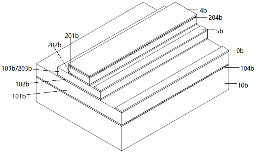
[0055] This embodiment introduces an AlGaInAs / InP multi-junction distributed feedback semiconductor laser (DFB-LD) with a wavelength of 1550 nm.

[0056] Such as image 3 As shown, the following materials are epitaxially grown once on a highly doped p-type InP substrate 10b: the grating layer 104b of the first PN junction is a p-type InGaAsP layer (thickness 10nm, doping concentration 1×10 18 cm -3 ).

[0057] The grating pattern formation process is as follows: on the basis of a primary epitaxial structure, a photoresist with a period range of 230-250nm first-order grating is formed by holographic interference lithography, electron beam lithography, nanoimprinting or projection lithography pattern. The grating pattern is transferred from the photoresist to the grating layer 104b of the first PN junction, that is, the p-type InGaAsP layer, by wet or dry etching technology.

[0058] After the grating pattern is made, the second epitaxial growth is performed, and the first P...

specific preparation Embodiment 3

[0067] This embodiment introduces an AlGaInAs / InP multi-junction distributed feedback semiconductor laser (DFB-LD) with a wavelength of 1310 nm.

[0068] refer to figure 2 , on a highly doped n-type InP substrate 10a, the following materials are epitaxially grown from bottom to top: the first PN junction N region 101a is an n-type InP buffer layer (thickness 500nm, doping concentration about 1×10 18 cm -3 ); the light-emitting region 102a of the first PN junction, the light-emitting region 102a comprises from bottom to top: non-doped lattice matching AlGaInAs lower waveguide layer (thickness 50nm, light fluorescence wavelength 1050nm), AlGaInAs active layer multiple quantum wells (2 For quantum wells, well width 8nm, 1% compressive strain, photofluorescent wavelength 1460nm, barrier width 10nm, 0.2% tensile strain, photofluorescent wavelength 1050nm), non-doped lattice matching AlGaInAs upper waveguide layer (thickness 20nm, photoluminescence wavelength 1050nm); the first P...


PUM

PropertyMeasurementUnit
wavelengthaaaaaaaaaa
thicknessaaaaaaaaaa
wavelengthaaaaaaaaaa

Abstract

The invention provides a multi-junction distributed feedback semiconductor laser. The laser comprises a substrate and a laser DFB-LD functional layer growing on the surface of the substrate; the DFB-LD functional layer comprises a plurality of semiconductor PN junctions and a grating; the plurality of semiconductor PN junctions are distributed up and down and are electrically connected with each other, and a junction region of each PN junction is provided with a light-emitting region; and the grating is positioned on any one of the semiconductor PN junctions or a connecting layer between the semiconductor PN junctions. According to the DFB-LD, the effective light emitting area of the laser can be increased, the symmetry of the transverse light field distribution of the waveguide cross section is improved, and the parasitic capacitance parameter of the laser is reduced, so that the laser has the advantages of high power, high modulation rate and high optical fiber coupling efficiency.

Description

technical field [0001] The present application relates to the technical field of semiconductor lasers, in particular to a multi-junction distributed feedback semiconductor laser. Background technique [0002] High power, high modulation rate single-mode semiconductor lasers are widely used in civil and military fields. In the field of digital optical fiber communication, high modulation rate single-mode semiconductor laser has become an indispensable light source. In recent years, high-power, high-modulation rate single-mode semiconductor lasers have also been widely used in military and civilian fields such as microwave photonics and atomic clocks. Compared with traditional digital optical fiber communication, new application scenarios such as microwave photonics, atomic clocks, and coherent optical communication have put forward new requirements for the performance of single-mode semiconductor lasers, such as power characteristics. Research and design high-power, high-mo...

Claims


Application Information

Patent Timeline
Patent Type & Authority Applications(China)
IPC IPC(8): H01S5/323H01S5/343H01S5/12
CPCH01S5/1228H01S5/3235H01S5/32391H01S5/34306H01S2304/00
Inventor 罗毅王健
Owner TSINGHUA UNIV
Why Eureka
Try Eureka