Grid electrode-enhanced surface plasmon laser and preparation method thereof

A surface plasmon and laser technology, applied in lasers, laser components, semiconductor lasers, etc., can solve the problem that the size cannot break through the optical diffraction limit

Active Publication Date: 2022-07-12
NANJING UNIV
View PDF6 Cites 0 Cited by
  • Summary
  • Abstract
  • Description
  • Claims
  • Application Information

AI Technical Summary

Problems solved by technology

However, the size of the above-mentioned lasers cannot break through the limitation of the optical diffraction limit, and further exploration is needed to achieve ultra-small size and ultra-low threshold.

Method used


Image

  • Grid electrode-enhanced surface plasmon laser and preparation method thereof
  • Grid electrode-enhanced surface plasmon laser and preparation method thereof
  • Grid electrode-enhanced surface plasmon laser and preparation method thereof

Examples


Embodiment 1

[0050] Embodiment 1 A grid electrode enhanced surface plasmon laser.

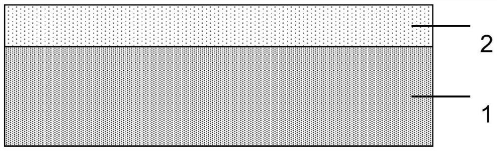
[0051] In this example, the substrate material is silicon wafer 1, and the specific preparation method of a grid electrode-enhanced surface plasmon laser is as follows:

[0052] (1) If figure 1 As shown, a layer of 200 nm thick SiO was deposited on the silicon wafer 1 by means of plasma-enhanced chemical vapor deposition (PECVD) technology. 2 Insulating layer 2, PECVD grown SiO 2 The way is to pass 5% SiH into the reaction chamber 4 / N 2 and N 2 The mixed gas of O, the flow rate is 100sccm and 450sccm respectively, under the conditions of pressure 300mTorr, power 10W, temperature 350℃, through SiH x +O→SiO 2 (+H 2 ) reaction to deposit SiO on the surface of epitaxial wafer 2 , the time is 9 minutes and 40 seconds;

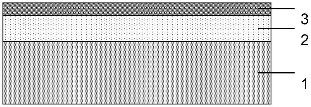
[0053] (2) If figure 2 shown in the first insulating layer of SiO 2 A silver (Ag) metal layer 3 with a thickness of 80 nm is deposited on the surface of the layer 2 by a physical vap...


PUM

PropertyMeasurementUnit
thicknessaaaaaaaaaa
widthaaaaaaaaaa
thicknessaaaaaaaaaa

Abstract

The invention discloses a grid electrode-enhanced surface plasmon laser, which comprises a surface plasmon substrate, a multi-quantum well nanowire and a grid electrode. In the invention, the grid electrode is used to stimulate the nanostructure by electromagnetic field, and the plasmon can form resonance coupling with the excitons in the gain medium to realize the stimulated radiation of photons in the gain medium, and the enhanced surface plasmon excitation is successfully obtained. The core of the nano-laser is to stimulate the carriers in the nano-optical cavity by using the grid electrode to stimulate the carrier in the nano-optical cavity, thereby enhancing the excitation of light in the nano-optical cavity and reducing the threshold of the surface plasmon laser. 0.8W / cm at room temperature 2 Low-threshold lasing improves the quality factor Q value of the laser. The present invention is characterized in that the grid electrode has no contact with the nano-optical cavity, effectively avoids the leakage problem while implementing the electromagnetic field loading, and can break through the limitation of the optical diffraction limit in one dimension.

Description

technical field [0001] The invention relates to a grid electrode-enhanced surface plasmon laser structure and a preparation method thereof, belonging to the technical field of lasers. Background technique [0002] Since its inception, lasers have had important applications in industrial, medical, military and other fields. In recent years, laser technology and applications have developed rapidly and have been combined with multiple disciplines to form multiple application technology fields. [0003] Such as optoelectronic technology, laser medicine and photonic biology. However, the above-mentioned lasers cannot break through the optical diffraction limit in size, and further exploration is needed to achieve ultra-small size and ultra-low threshold. In 2003, Bergman and Stockman first proposed the basic idea of ​​plasmon amplification of stimulated radiation at subwavelength scale. The lasing of nanolasers with a threshold of 76.25MW / cm 2 , has received extensive attenti...

Claims


Application Information

Patent Timeline
Patent Type & Authority Patents(China)
IPC IPC(8): H01S5/042H01S5/34
CPCH01S5/04254H01S5/04252H01S5/341
Inventor 陶涛苗涛蒋迪智婷刘斌
Owner NANJING UNIV
Why Eureka
Try Eureka