VCSEL chip and preparation method thereof

A chip and silicon nitride layer technology, applied in laser parts, electrical components, lasers, etc., can solve the problems of attenuation, chip efficiency reduction, influence of chip resistance value, etc., to reduce internal resistance and improve optical performance. Effect

Pending Publication Date: 2021-09-28
威科赛乐微电子股份有限公司
View PDF0 Cites 0 Cited by
  • Summary
  • Abstract
  • Description
  • Claims
  • Application Information

AI Technical Summary

Problems solved by technology

[0003] As a semiconductor laser, VCSEL excites the semiconductor electrons to jump from the valence band to the conduction band. When the electrons jump back from the conduction band to the valence band, the energy is released in the form of light energy, such as figure 1 As shown, the traditional VCSEL chip structure includes substrate, N-DBR, MQW active layer, oxide layer, P-DBR, P-contact and P-ohmic (P-ohmic contact) from bottom to top, traditional VCSEL, When growing epitaxy, 10 to 20 pairs of P-DBRs made of AlGaAs will be grown on the MQW active layer. Due to the large number of P-DBRs, it will affect the resistance value of the chip, and the current must pass through so many DBRs. In order to reach the MQW active layer to play a role, it is attenuated in the process, which greatly reduces the efficiency of the chip

Method used


Image

  • VCSEL chip and preparation method thereof
  • VCSEL chip and preparation method thereof
  • VCSEL chip and preparation method thereof

Examples


Embodiment 1

[0029] The preparation method of the above-mentioned high-efficiency VCSEL chip is as follows:

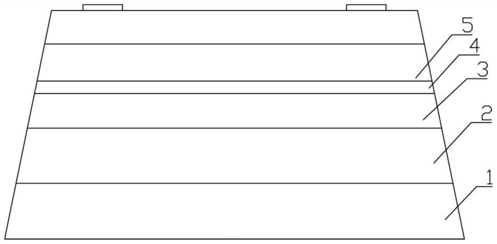
[0030] S1: GaAs substrate 1 is provided, and N-DBR structure 2, MQW active layer 3, oxide layer 4 and P-DBR structure 5 are sequentially grown on GaAs substrate 1 according to conventional methods;

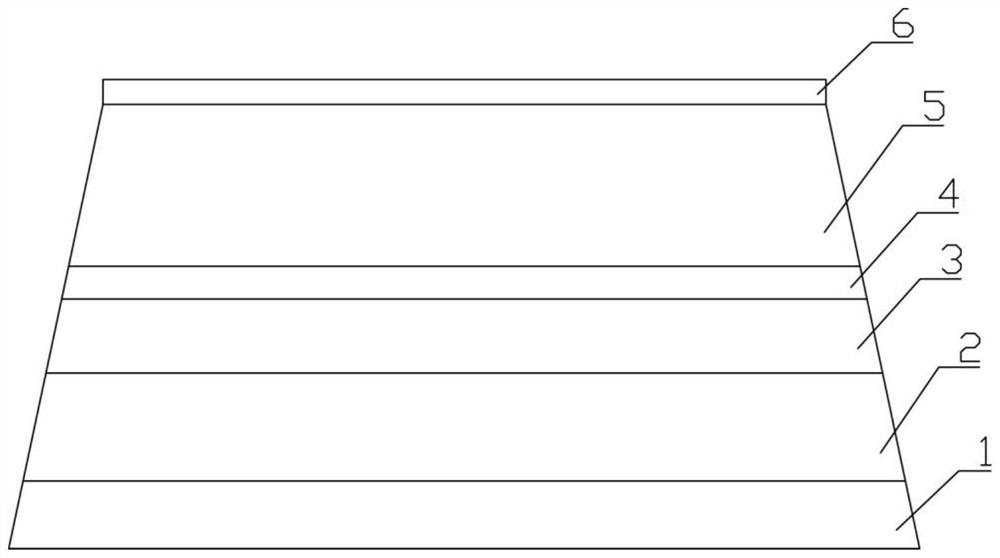
[0031] S2: Using a PECVD machine to deposit silicon nitride on the P-DBR to form the first silicon nitride layer 6 by conventional methods, such as figure 2 shown;

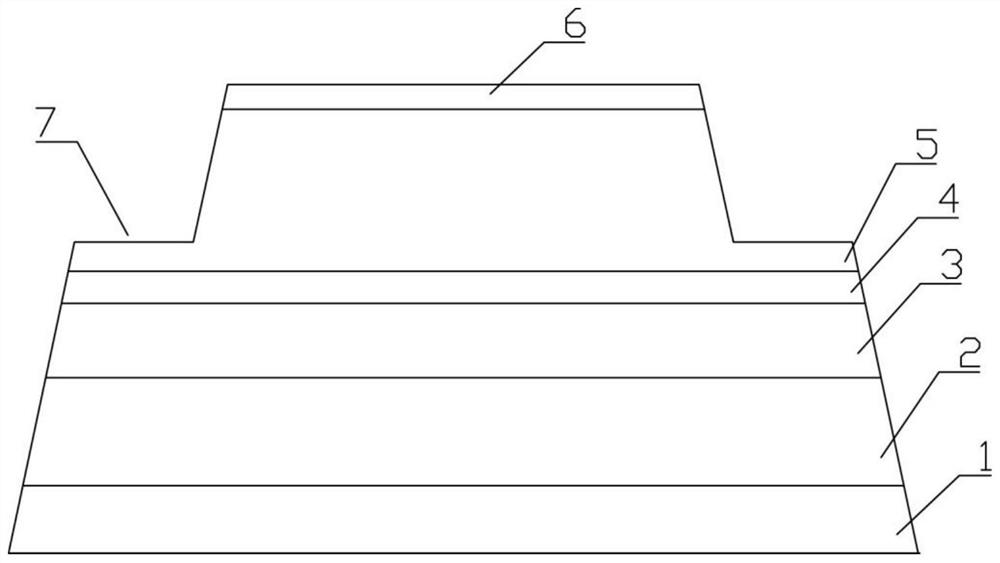
[0032] S3: if image 3 As shown, the first silicon nitride layer 6 and the P-DBR structure 5 are etched until the P-DBR structure 5 has 2-3 pairs of DBR layers left to form a mesa 7;

[0033] S4: if Figure 4 As shown, C or Ge material is deposited on the mesa 7 to obtain a P-contact ring 8;

[0034] S5: if Figure 5 As shown, the second silicon nitride layer 9 is obtained by depositing silicon nitride from the GaAs substrate 1 up to the first silicon nitride layer 6 according to a conventional method;

[0035] S6: ...

Embodiment 2

[0038] In addition, the P-contact ring 8 can also be obtained through secondary epitaxy of a highly doped layer. The specific method is as follows:

[0039] S1: GaAs substrate 1 is provided, and N-DBR structure 2, MQW active layer 3, oxide layer 4 and P-DBR structure 5 are sequentially grown on GaAs substrate 1;

[0040] S2: Depositing silicon nitride on the P-DBR to form a first silicon nitride layer 6;

[0041] S3: Etching the first silicon nitride layer 6 and the P-DBR structure 5 until the P-DBR structure 5 has 2-3 pairs of DBR layers left to form the mesa 7;

[0042] S4: A P-contact ring 8 is obtained by secondary epitaxial highly doped layer on the mesa 7;

[0043] S5: Etching away the highly doped layer other than the P-contact ring 8, and then depositing silicon nitride from the GaAs substrate 1 up to the first silicon nitride layer 6 to obtain the second silicon nitride layer 9;

[0044] S6: Etching the second silicon nitride layer 9 to the P-contact ring 8 to obtai...


PUM


Abstract

The invention discloses a VCSEL chip and a preparation method thereof, and relates to the technical field of laser chips. The VCSEL chip comprises a substrate and an epitaxial structure located on one side of the substrate, the epitaxial structure comprises an N-DBR structure, an MQW active layer, an oxide layer and a P-DBR structure which are sequentially deposited from bottom to top, a first silicon nitride layer is deposited on the P-DBR structure, the first silicon nitride layer and the P-DBR structure are etched downwards to form a table top, a P-contact circular ring is arranged on the table top, a second silicon nitride layer is deposited on the substrate upwards to the first silicon nitride layer, and P-ohmic is formed on the second silicon nitride layer at the position corresponding to the P-contact circular ring through vapor plating. According to the VCSEL chip and the preparation method thereof, the internal resistance of the chip can be effectively reduced by reducing the distance from P-contact to an MQW active layer, the optical performance of the chip is improved, and the efficiency is improved.

Description

technical field [0001] The invention relates to the technical field of laser chips, in particular to a VCSEL chip and a preparation method thereof. Background technique [0002] VCSEL, full name vertical cavity surface emitting laser, is developed on the basis of gallium arsenide semiconductor materials. It is different from other light sources such as LED and LD (laser diode), with small size, circular output spot, single longitudinal mode output, threshold With the advantages of low current, low price, and easy integration into large-area arrays, it is widely used in optical communication, optical interconnection, optical storage and other fields. [0003] As a semiconductor laser, VCSEL excites the semiconductor electrons to jump from the valence band to the conduction band. When the electrons jump back from the conduction band to the valence band, the energy is released in the form of light energy, such as figure 1 As shown, the traditional VCSEL chip structure includes...

Claims


Application Information

Patent Timeline
Patent Type & Authority Applications(China)
IPC IPC(8): H01S5/183H01S5/34
CPCH01S5/18361H01S5/18344H01S5/34
Inventor 彭鹏姚林松张健
Owner 威科赛乐微电子股份有限公司
Why Eureka
Try Eureka