Terahertz modulator based on graphene/boron nitride heterostructure and preparation method thereof

A heterostructure, boron nitride technology, applied in the field of terahertz wave applications, can solve the problems of influence, small optical modulation depth, low efficiency, etc., achieve strong modulation capability, improve optical modulation depth and speed, and increase carriers. The effect of mobility

Pending Publication Date: 2021-10-12
UNIV OF ELECTRONICS SCI & TECH OF CHINA +1
View PDF0 Cites 0 Cited by
  • Summary
  • Abstract
  • Description
  • Claims
  • Application Information

AI Technical Summary

Problems solved by technology

However, in semiconductors, the efficiency of laser excitation is low, resulting in a small depth of light modulation, which affects practical applications. At present, there is an urgent need to improve the light modulation depth and speed of semiconductors for terahertz waves.

Method used


Image

  • Terahertz modulator based on graphene/boron nitride heterostructure and preparation method thereof
  • Terahertz modulator based on graphene/boron nitride heterostructure and preparation method thereof
  • Terahertz modulator based on graphene/boron nitride heterostructure and preparation method thereof

Examples


Embodiment 1

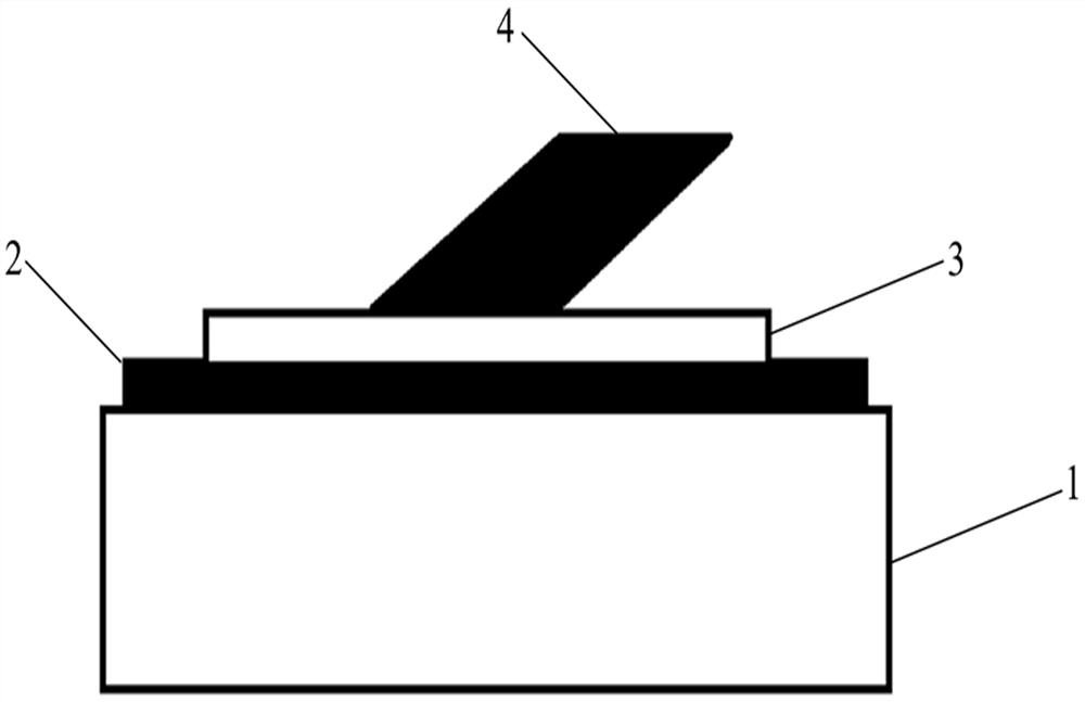
[0019] An embodiment of the present invention provides an optically controlled terahertz wave modulator based on a graphene / boron nitride heterostructure, figure 1 A schematic structural diagram of an optically controlled terahertz wave modulator based on a graphene / boron nitride heterostructure according to an embodiment of the present invention is shown, including a p-type silicon substrate 1, a boron nitride thin film 2, Graphene film 3 and infrared laser beam 4;

[0020] During the modulation process, the terahertz wave is incident vertically from one side of the graphene film 3, and the detector is received on the other side of the P-type silicon substrate 1; during optical modulation, the infrared laser beam 4 is incident at a certain angle (45° angle) to the graphene film side to achieve optical modulation. Due to its large band gap and small thickness, the introduction of boron nitride film will further effectively separate the photogenerated electrons and holes, prev...

Embodiment approach

[0024] As a specific implementation manner, the resistivity of the P-type silicon substrate 1 is 10-30 Ω•cm, and the thickness of the P-type silicon substrate is 400-600 μm.

[0025] As a specific implementation manner, the resistivity of the graphene film 3 is 100-3000Ω·cm.

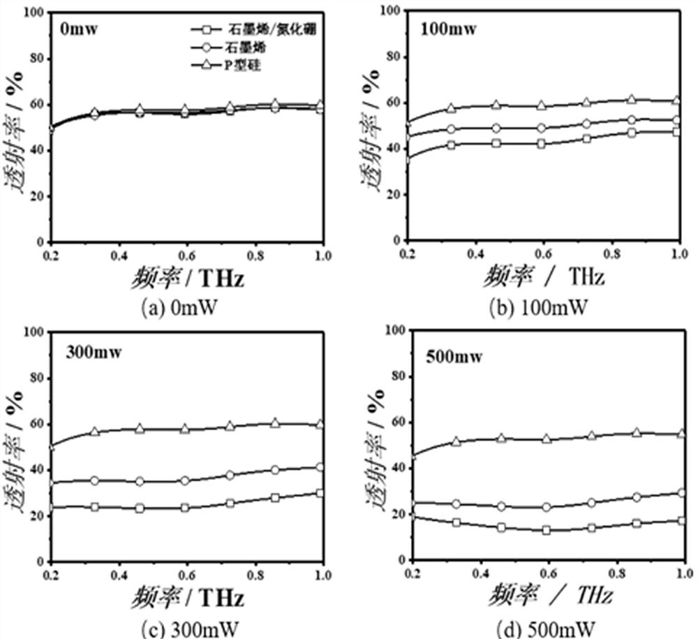
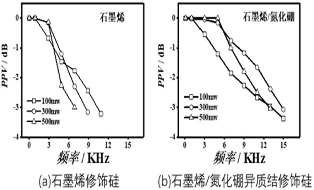
[0026] A terahertz modulator based on a graphene / boron nitride heterostructure provided by the present invention, the terahertz wave modulator includes a p-type silicon substrate, a boron nitride film, and a graphene film arranged in sequence from bottom to top As well as infrared laser beams, compared with conventional graphene film-modified terahertz modulators, boron nitride films can greatly increase the carrier mobility of graphene films, graphene / boron nitride heterostructures and single-layer graphite Compared with the graphene-modified silicon structure, the carrier mobility of the graphene-modified silicon is much higher. Under the irradiation of the same power laser, the internal carrier mobili...

Embodiment 2

[0028] An embodiment of the present invention provides a method for preparing an optically controlled terahertz wave modulator based on a graphene / boron nitride heterostructure. The terahertz wave modulator is prepared by the following steps:

[0029] Step 1. Cut the single-oxide layer p-type silicon wafer (100) with a front oxide layer thickness of 100nm and a resistivity between 10-30 Ω·cm into square pieces of 10mm×10mm, and use acetone, alcohol, and deionized The water is cleaned in ultrasonic, and dried with nitrogen gas to obtain a clean silicon wafer;

[0030] Step 2, transfer boron nitride film:

[0031] Cut the copper substrate with boron nitride film obtained by CVD into a size of 9mm×9mm, spin-coat a layer of PMMA on the side where the boron nitride film grows, and then put 1mol / L FeCl 3 The copper substrate was corroded in the solution. After standing for 3 hours, a layer of transparent film (PMMA) floating on the surface of the solution was observed, which proved...


PUM

PropertyMeasurementUnit
electrical resistivityaaaaaaaaaa
thicknessaaaaaaaaaa
electrical resistivityaaaaaaaaaa

Abstract

The invention provides a terahertz modulator based on a graphene/boron nitride heterostructure and a preparation method thereof, and the terahertz modulator comprises a p-type silicon substrate, a boron nitride thin film, a graphene thin film and an infrared laser beam which are sequentially arranged from bottom to top. Compared with a conventional terahertz modulator modified by a graphene thin film, the boron nitride thin film can greatly increase the carrier mobility of the graphene thin film, compared with a single-layer graphene modified silicon structure, the graphene/boron nitride heterostructure has the carrier mobility far higher than that of graphene modified silicon, and under irradiation of laser with the same power, the terahertz modulator with boron nitride as the insulating layer is higher in internal carrier mobility, through the combined action of boron nitride and graphene, the light modulation depth and speed of terahertz waves are improved under the excitation of infrared laser, and the terahertz modulator is higher in terahertz wave modulation capacity.

Description

technical field [0001] The invention belongs to the technical field of terahertz wave applications, and relates to a terahertz wave modulator and a preparation method thereof, in particular to a graphene / boron nitride heterostructure-based terahertz modulator and a preparation method thereof. Background technique [0002] Terahertz wave (THz Wave) is an electromagnetic wave between microwave and infrared light, which has great application prospects in security inspection, high-speed communication, non-destructive imaging and other fields. A terahertz wave modulator is an electronic device that can controlly modulate the intensity or phase of a terahertz wave, and plays an important role in many terahertz wave technologies. For low-speed, broadband and low-loss terahertz wave modulator applications, such as terahertz spatial modulators used in terahertz compressive sensing imaging, the dynamic process of generation and recombination of photogenerated carriers in semiconduct...

Claims


Application Information

Patent Timeline
Patent Type & Authority Applications(China)
IPC IPC(8): G02F1/015C01B21/064C01B32/194
CPCG02F1/015C01B21/0648C01B32/194
Inventor 文天龙王卓然
Owner UNIV OF ELECTRONICS SCI & TECH OF CHINA
Why Eureka
Try Eureka