Base bias voltage adjusting device and method and semiconductor process equipment

A bias voltage adjustment and susceptor technology, which is applied in semiconductor/solid-state device manufacturing, metal material coating process, vacuum evaporation plating, etc., can solve problems such as small process window, damaged wafer, unqualified process results, etc., to achieve The effect of expanding the process window, avoiding mutual interference, and expanding the adjustment range

Active Publication Date: 2021-11-05
BEIJING NAURA MICROELECTRONICS EQUIP CO LTD
View PDF6 Cites 1 Cited by
  • Summary
  • Abstract
  • Description
  • Claims
  • Application Information

AI Technical Summary

Problems solved by technology

[0005] However, since the aforementioned RF power supply 05 can only apply negative bias voltage to the susceptor 03, the wafer may be damaged in some processes, resulting in an excessively high forward voltage (Voltage Forward, VF) value of the wafer, resulting in poor process results. qualified
Moreover, the process window of the PVD equipment is small, which cannot meet the needs of different processes

Method used


Image

  • Base bias voltage adjusting device and method and semiconductor process equipment
  • Base bias voltage adjusting device and method and semiconductor process equipment
  • Base bias voltage adjusting device and method and semiconductor process equipment

Examples


no. 1 example

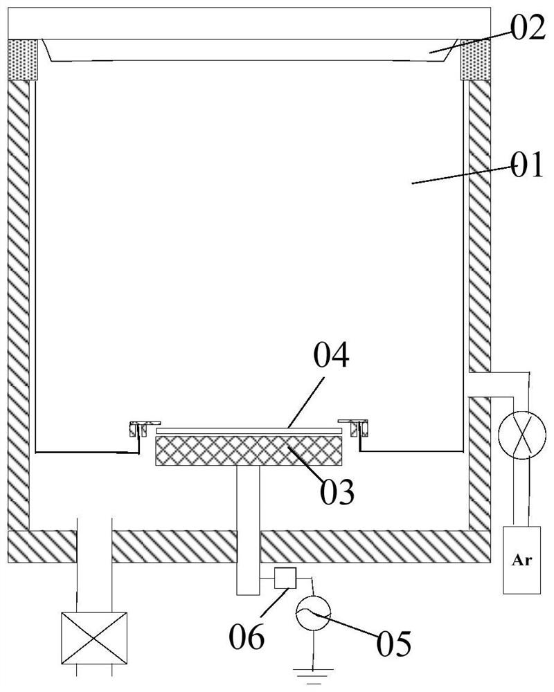
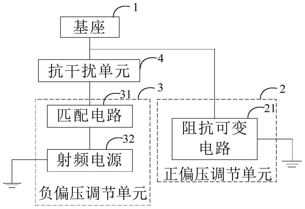
[0057] see figure 2 , the base bias adjustment device provided by the first embodiment of the present invention, which includes a positive bias adjustment unit 2, a negative bias adjustment unit 3 and an anti-interference unit 4, wherein the first end of the positive bias adjustment unit 2 is grounded , the second end is connected to the base 1, the positive bias adjustment unit 2 is used to adjust the bias voltage of the base 1, and can make the base 1 generate a positive bias; the first end of the negative bias adjustment unit 3 is grounded, the second The two ends are connected with the base 1 for adjusting the bias voltage of the base 1 and enabling the base 1 to generate a negative bias voltage. The anti-interference unit 4 is connected to the circuit between the negative bias adjustment unit 3 and the base 1, and is used to suppress the current in the circuit between the positive bias adjustment unit 2 and the base 1 from flowing into the negative bias adjustment unit 3...

no. 2 example

[0072] see Figure 5, The base bias adjustment device provided by the second embodiment of the present invention is an improvement on the base bias adjustment device based on the first embodiment above. Specifically, on the basis of the above-mentioned first embodiment, the susceptor bias adjustment device further includes a parameter acquisition unit and a control unit 53, wherein the parameter acquisition unit is used to acquire the impedance-related current of the forward bias adjustment unit 2 in real time. parameter value and send it to the control unit 53. The above-mentioned current parameter values ​​related to impedance are, for example, the current bias voltage value of the base 1 or the input voltage value and input current value (from the base 1 ) of the forward bias voltage adjustment unit 2 and so on. The control unit 53 is used to control the positive bias voltage adjusting unit 2 to adjust the bias voltage of the base 1 according to the above-mentioned current...

no. 3 example

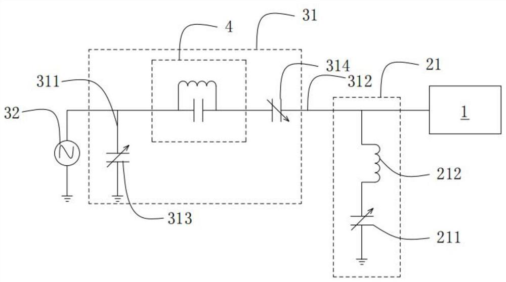
[0079] see Figure 6 , the base bias adjustment device provided by the third embodiment of the present invention, compared with the above-mentioned first and second embodiments, the difference is that: the impedance variable circuit 21' is the same as that of the above-mentioned first and second embodiments The variable impedance circuit 21 is different.

[0080] Specifically, the variable impedance circuit 21' also includes a first variable capacitor 211, by adjusting the capacitance value of the first variable capacitor 211, the impedance of the variable impedance circuit 21 can be adjusted, thereby realizing the bias voltage of the base 1 adjustment. On this basis, according to different process conditions and process requirements, corresponding fixed capacitance and / or fixed inductance can be set in the impedance variable circuit 21, for example, as Figure 6 As shown, a fixed inductance 212 connected in parallel with the first variable capacitor 211 is also provided in ...


PUM


Abstract

The invention provides a base bias voltage adjusting device and method and semiconductor process equipment. The device comprises a positive bias voltage adjusting unit, a negative bias voltage adjusting unit and an anti-interference unit, wherein the first end of the positive bias voltage adjusting unit is grounded, the second end of the positive bias voltage adjusting unit is electrically connected with a base, the positive bias voltage adjusting unit is used for adjusting the bias voltage of the base, and the base can generate positive bias voltage; the first end of the negative bias voltage adjusting unit is grounded, the second end of the negative bias voltage adjusting unit is electrically connected with the base, and the negative bias voltage adjusting unit is used for adjusting bias voltage of the base, and the base can generate negative bias voltage; and the anti-interference unit is connected to a circuit between the negative bias voltage adjusting unit and the base and used for inhibiting current in a circuit between the positive bias voltage adjusting unit and the base from flowing into the circuit between the negative bias voltage adjusting unit and the base. According to the technical scheme of the base bias voltage adjusting device and method and the semiconductor process equipment provided by the invention, different process requirements can be met, so that a process window is expanded.

Description

technical field [0001] The present invention relates to the technical field of semiconductor manufacturing, in particular to a base bias adjustment device and method, and semiconductor process equipment. Background technique [0002] Plasma is widely used in the production process of semiconductor devices. In a plasma etching or deposition system, an RF power source is used to excite the process gas in the reaction chamber to generate plasma. The plasma contains a large number of active particles such as electrons, ions, excited atoms, molecules and free radicals. These active particles interact with the wafer placed in the reaction chamber and exposed to the plasma environment, causing the surface of the wafer to Various physical and chemical reactions to complete the etching of the wafer or other processes. [0003] Since electrons are lighter than positive ions, more electrons fall on the surface of the wafer than ions in the same time period, thus forming a DC negative...

Claims


Application Information

Patent Timeline
Patent Type & Authority Applications(China)
IPC IPC(8): C23C14/54C23C14/56H01L21/67
CPCC23C14/542C23C14/56H01L21/67253
Inventor 张超
Owner BEIJING NAURA MICROELECTRONICS EQUIP CO LTD
Why Eureka
Try Eureka