Integrated structure of chip and substrate antenna based on flip process

A flip-chip and flip-chip technology, which is applied in the field of integrated structures based on flip-chip technology chips and substrate antennas, can solve the problems of inability to solve chip heat dissipation, inability to adapt to RF chips, and high external dimensions, and achieve miniaturized wireless Transceiver function, realize wireless transceiver function, reduce the effect of high-frequency signal transmission path

Pending Publication Date: 2021-11-09
BEIJING 7Q TECH
View PDF2 Cites 2 Cited by
  • Summary
  • Abstract
  • Description
  • Claims
  • Application Information

AI Technical Summary

Problems solved by technology

[0006] The above-mentioned first example, Chinese Invention Patent Publication No. CN101057327A is aimed at ID (identity) chip, which realizes the integrated manufacturing process with film antenna; Most general-purpose RF chips or SoCs (digital-analog hybrid chips) with a large scale and area cannot solve problems such as chip heat dissipation.
[0007] The second example above, Chinese Utility Model Patent Publication No. ZL201920060815.7 discloses a chip antenna unitary structure based on a multi-layer recessed substrate; It is also suitable for most large-scale general-purpose RF chips or SoCs (digital-analog hybrid chips), but the biggest disadvantage of the integrated structure of such chips and antennas is the height of the overall size of the integrated structure. Relatively high, relatively poor heat dissipation

Method used


Image

  • Integrated structure of chip and substrate antenna based on flip process
  • Integrated structure of chip and substrate antenna based on flip process

Examples


Embodiment 1

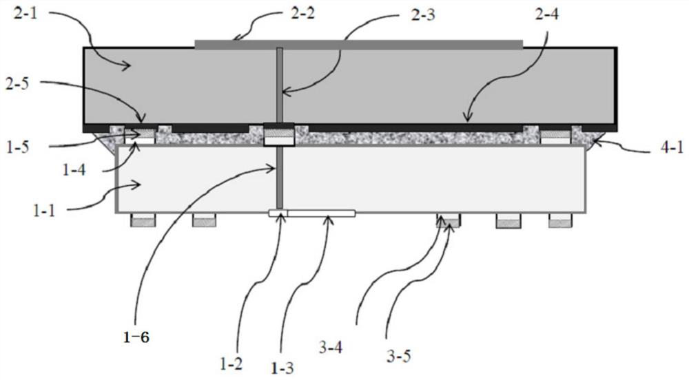
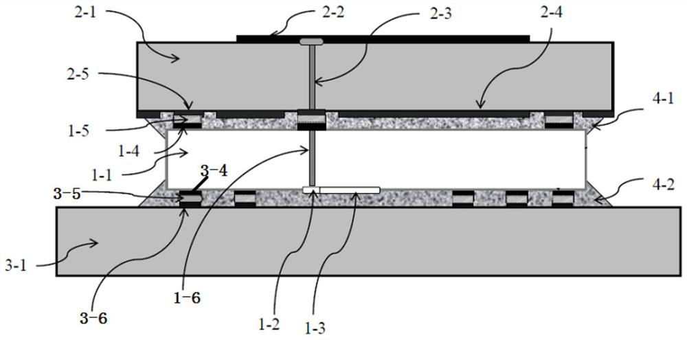
[0039] Wireless-enabled devices are inseparable from high-frequency chips and antennas. While the chip needs reliability protection, the antenna needs to be as directly open as possible to transmit or receive signals into the air. The current open and separated connection installation structure is susceptible to radiation interference from other signals. The patent of the present invention relates to an integrated structure based on a flip-chip chip and a substrate antenna. On the basis of including a high-frequency chip, the electrodes of the input and output ends of the high-frequency chip are integrated by using flip-chip FC and semiconductor TSV through-hole technology. The TSV is connected to the feed end of the antenna substrate, and after the high-frequency chip and the electrode of the antenna substrate are welded, glue is filled between the two to form a stable protection and integrated structure; finally, the flip chip and the substrate antenna are integrated The opt...


PUM


Abstract

The invention relates to an integrated structure of a chip and a substrate antenna based on a flip process. The integrated structure comprises a flip chip 1-1, a connecting base plate 1-2, a high-frequency circuit 1-3, an antenna substrate 2-1, an antenna surface structure 2-2, an antenna feed hole 2-3 and a TSV through hole 1-6. The flip chip 1-1 is located below the antenna substrate 2-1, the antenna feed hole 2-3 penetrates through the antenna substrate 2-1, and the TSV through hole 1-6 penetrates through the flip chip 1-1; the connecting base plate 1-2 and the high-frequency circuit 1-3 are both located on the lower surface of the flip chip 1-1 and electrically connected, the antenna surface structure 2-2 is located on the upper surface of the antenna substrate 2-1, and the antenna surface structure 2-2 is connected with the connecting base plate 1-2 through an antenna feed hole 2-3 and a TSV through hole 1-6. Extremely small path loss between a high-frequency device and the antenna is reduced, and meanwhile, the requirements of a small-size structure and high performance are met.

Description

technical field [0001] The invention relates to a new design and layout of a wireless chip, relates to the structural design of a flip chip and a TSV through hole, and organically combines the other side of the flip chip with an antenna substrate to form an integrated structure. In particular, the organic combination of flip chip, TSV through hole and substrate antenna involves the intersection of chip design and manufacturing, packaging and wireless antenna technology. Background technique [0002] Up to now, various devices and terminals related to electronic information systems have been required to be miniaturized and integrated depending on the application. So far, the chip is usually installed on the mother substrate, and the independent design is installed outside the mother substrate (represented by the rod antenna) or on the mother substrate (represented by the microstrip antenna and the surface-mounted dielectric antenna). However, in the previous chip packages, w...

Claims


Application Information

Patent Timeline
Patent Type & Authority Applications(China)
IPC IPC(8): H01L23/66H01L23/538H01L23/367H01Q1/22
CPCH01L23/66H01L23/5384H01L23/5386H01L23/3677H01Q1/2283
Inventor 阎跃鹏
Owner BEIJING 7Q TECH
Why Eureka
Try Eureka