Shadow mask for patterned vapor deposition of organic light emitting diode (OLED) material, shadow mask module comprising same and method for manufacturing shadow mask module

A technology of light-emitting diodes and patterning, which is applied to photosensitive materials used in optomechanical equipment, photoplate-making process of pattern surface, metal material coating process, etc., which can solve alignment and alignment errors, inhomogeneity, Solve problems such as film bending, achieve high yield, reliable manufacturing process, and enhance mechanical strength and flatness

Pending Publication Date: 2021-11-19
THE HONG KONG UNIV OF SCI & TECH
View PDF1 Cites 2 Cited by
  • Summary
  • Abstract
  • Description
  • Claims
  • Application Information

AI Technical Summary

Problems solved by technology

However, the same tensile stress also creates a force that pulls the silicon frame inward, causing the film to bend
As a result, there is an unwanted gap between the shadow mask and the substrate, causing alignment and misalignment errors between the two masks, and significant shifts and non-uniformities in the deposited pattern

Method used


Image

  • Shadow mask for patterned vapor deposition of organic light emitting diode (OLED) material, shadow mask module comprising same and method for manufacturing shadow mask module
  • Shadow mask for patterned vapor deposition of organic light emitting diode (OLED) material, shadow mask module comprising same and method for manufacturing shadow mask module
  • Shadow mask for patterned vapor deposition of organic light emitting diode (OLED) material, shadow mask module comprising same and method for manufacturing shadow mask module

Examples


Embodiment 1

[0055] In this embodiment, the fabrication process of a shadow mask according to the structure disclosed in the disclosed method is described.

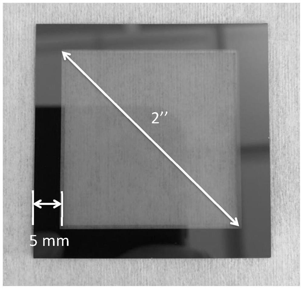
[0056] A 4-inch double-sided polished silicon wafer with a thickness of 400 μm was used as a starting substrate to fabricate a shadow mask. Sequentially use deionized water and 120°C sulfuric acid solution (sulfuric acid H 2 SO 4 / hydrogen peroxide H 2 o 2 =10 / 1) After cleaning, the wafer was immersed in a hydrofluoric acid (HF) solution at room temperature for 1 minute to remove native oxide. The wafer is then transferred to a furnace where both sides of the wafer are grown at a temperature of 1000°C of silicon oxide (SiOx). The silicon oxide on one side of the wafer is removed by an oxide etchant. The other side of the wafer that still has silicon oxide on it is defined as the front side, while the side without silicon oxide is defined as the back side. Next, 1.5 μm silicon nitride (SiN x ). Photoresist was then spin-coate...

Embodiment 2

[0058] A shadow mask was produced in the same manner as in Example 1, except that the thickness of the silicon oxide layer was instead of

Embodiment 3

[0060] A shadow mask was produced in the same manner as in Example 1, except that the thickness of the silicon oxide layer was instead of


PUM

PropertyMeasurementUnit
thicknessaaaaaaaaaa
lengthaaaaaaaaaa
thicknessaaaaaaaaaa

Abstract

The invention relates to a shadow mask and a shadow mask module for organic light emitting diode (OLED) material patterning vapor deposition. The shadow mask includes a ceramic membrane under tensile stress, the ceramic membrane including a central membrane region having a plurality of through holes. The through holes form a hole array, so that the vaporized deposition material can pass through the hole array. A peripheral membrane region surrounds the central membrane region. A multi-layer peripheral support is attached to the rear surface of the peripheral membrane region and has a hollow portion below the central membrane region. The multi-layer peripheral support has a base layer and an intermediate layer under compressive stress over the base layer and attached to the lower surface of the peripheral membrane region. The compressive stress of the intermediate layer is selected to balance the tensile stress of the ceramic membrane such that the ceramic membrane remains in a planar state. A shadow mask module includes a rigid carrier having a plurality of support windows and a plurality of shadow masks attached to the support windows.

Description

technical field [0001] The present invention relates generally to shadow masks, and more particularly to high resolution shadow masks useful for patterned vapor deposition of organic light emitting diode (OLED) materials. The shadow mask is thin and flat due to balanced film stress. Background technique [0002] Shadow masking is an important patterning technique in the manufacture of semiconductor devices. In this process, the material to be patterned is evaporated or sublimated into a gas phase and then deposited onto the substrate through a shadow mask with a specific pattern of apertures that allows the material vapor to pass through. Fine shadow masks are especially important in the manufacture of full-color OLED displays. OLED display fabrication involves forming a patterned self-emitting organic film to produce individual red, green and blue (RGB) colors. OLEDs were first invented at Kodak Research Laboratories in 1987 and sparked extensive research efforts worldwi...

Claims


Application Information

Patent Timeline
Patent Type & Authority Applications(China)
IPC IPC(8): H01L51/56C23C14/04C23C16/04
CPCC23C14/042C23C16/042H10K71/164H10K71/166H10K71/00G03F7/12G03F7/0007G03F7/167G03F7/161G03F7/11G03F7/0041G03F7/0035B05C21/005H10K71/233
Inventor 董首成姜毅斌谭兆霆陆磊邓清云
Owner THE HONG KONG UNIV OF SCI & TECH
Why Eureka
Try Eureka