
Method for preparing indium arsenide/indium phosphide quantum dot laser epitaxial wafer with ultra-wide light emission spectrum

A technology of quantum dots and indium arsenide, which is applied in the field of preparing laser epitaxial wafers and indium arsenide/indium phosphide quantum dot laser epitaxial wafers with ultra-wide emission spectrum, which can solve the problem that the size distribution of quantum dots is difficult to control and the energy level is extremely high. Uniform broadening, unfavorable gain and other problems, to achieve the effect of wide applicability, simple steps, and convenient operation

Pending Publication Date: 2021-12-03
JIANGSU HUAXING LASER TECH CO LTD
View PDF10 Cites 0 Cited by
  • Summary
  • Abstract
  • Description
  • Claims
  • Application Information

AI Technical Summary

Problems solved by technology

[0005] However, in practice, quantum dots grown in SK mode have intrinsic size non-uniformity, which leads to non-uniform broadening of energy levels.
The size distribution of quantum dots grown by SK mode is difficult to control, and the spectrum has large non-uniform broadening (about 20-100 meV range or wider)
This is not conducive to the improvement of the gain of ordinary lasers with a specific wavelength

Method used


Image

  • Method for preparing indium arsenide/indium phosphide quantum dot laser epitaxial wafer with ultra-wide light emission spectrum
  • Method for preparing indium arsenide/indium phosphide quantum dot laser epitaxial wafer with ultra-wide light emission spectrum

Examples


Embodiment

[0027] Example: Sample 1

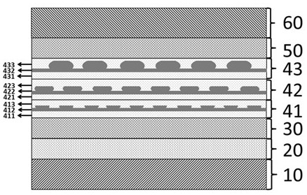
[0028] A method for preparing an indium arsenide / indium phosphide quantum dot laser epitaxial wafer with an ultra-broad emission spectrum, comprising the steps of:

[0029] Step 1: Select the substrate 10, which is n + type indium phosphide single wafer, the crystal orientation is (100), its doping element is Si, and the doping concentration is (1-3)×10 18 cm -3 .

[0030] Step 2: epitaxially grow a layer of indium phosphide buffer layer 20 on the indium phosphide substrate, the growth thickness of the indium phosphide buffer layer is 500nm, perform n-type doping on it, the doping element is Si element, doping The concentration is 1×10 18 cm -3 .

[0031] Step 3: Epitaxially grow InGaAsP lower confinement layers 30 on the InP buffer layer 20 with a growth thickness of 200 nm, which is an intrinsic material without doping.

[0032] Step 4: By controlling the deposition thickness of quantum dots and the thickness of the first capping layer, sta...


PUM

PropertyMeasurementUnit
Growth thicknessaaaaaaaaaa

Abstract

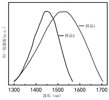
The invention discloses a method for preparing an indium arsenide / indium phosphide quantum dot laser epitaxial wafer with an ultra-wide light emission spectrum. The method comprises the following steps of: epitaxially growing a buffer layer and a lower respective limiting layer on an indium phosphide substrate; stacking and growing a plurality of quantum dot active layers; and depositing an upper respective limiting layer and an ohmic contact layer to finish the preparation. The size of the grown quantum dots is adjusted by controlling the deposition thickness of the quantum dots, and meanwhile, the height of the grown quantum dots is adjusted by adjusting the thickness of a first cover layer in two-step growth of quantum dot cover layers, so that stacked growth of the quantum dots with different sizes and heights is realized, and further the size and the height are adjusted to enable the prepared indium arsenide / indium phosphide quantum dot epitaxial wafer to have an ultra-wide light emission spectrum, the preparation method is simple in step, convenient to operate, controllable and adjustable, and the prepared epitaxial wafer is an ideal material for preparing a tunable laser and has very high practicability and wide applicability.

Description

technical field [0001] The invention relates to a method for preparing a laser epitaxial sheet, in particular to a method for preparing an ultra-wide emission spectrum indium arsenide / indium phosphide quantum dot laser epitaxial sheet, which belongs to the field of semiconductor technology. Background technique [0002] Semiconductor quantum dot lasers have unique advantages in realizing broadband tunability due to their low linewidth enhancement factor, high temperature stability, and ultrafast carrier dynamics. It has broad application prospects in the fields of optical fiber communication, biomedicine and environmental monitoring. [0003] Among several quantum dot materials, indium arsenide / gallium arsenide quantum dots with a wavelength of about 1.3 μm have attracted the most attention, and many good properties have been obtained due to the high growth quality of epitaxial materials. However, indium arsenide / gallium arsenide quantum dot materials are difficult to cover...

Claims


Application Information

Patent Timeline
IPC IPC(8): H01S5/34H01S5/343C30B29/40C30B25/18
CPCH01S5/3412H01S5/3434C30B29/40C30B25/183H01S2304/04H01S2304/02
Inventor 王岩徐鹏飞罗帅季海铭
Owner JIANGSU HUAXING LASER TECH CO LTD
Learn More