Electron transport material and organic electroluminescent device

An electron transport material, an unreplaced technology, applied in the field of organic electroluminescent devices, can solve the problems of high cost, instability, and many steps, and achieve the effects of high stability, high charge transfer ability, and high glass transition temperature

Inactive Publication Date: 2021-12-07
EVERDISPLAY OPTRONICS (SHANGHAI) CO LTD
View PDF0 Cites 0 Cited by
  • Summary
  • Abstract
  • Description
  • Claims
  • Application Information

AI Technical Summary

Problems solved by technology

For the choice of dopants, Lewis acid-type metal complexes, halogens, axenene, and quinones are relatively common, but metal complexes and halogens have disadvantages such as instability during device processing
However, axenic compounds have many steps in the synthesis, and the cost is relatively high.
Therefore, this method cannot improve the electron transport efficiency of organic electroluminescent devices very well.

Method used


Image

  • Electron transport material and organic electroluminescent device
  • Electron transport material and organic electroluminescent device
  • Electron transport material and organic electroluminescent device

Examples


Embodiment 1

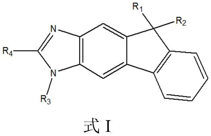
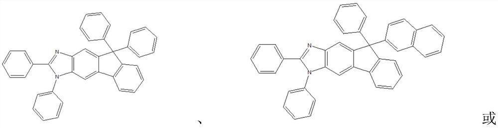
[0042] The synthetic method for preparing compound A is the same as the synthetic method for preparing the compound of formula I. The structures of compounds 2, 3, 4, 5 and 6 are

[0043]

[0044] The yield of compound A was 82%. Characterization data: melting point (DSC) 289°C, purity 99.9%; 1 H NMR (400MHz, CDCl 3 )δ (ppm): 8.06 (m, 1H), 7.80 (s, 1H), 7.61 (m, 1H), 7.56 (m, 1H), 7.48 (m, 2H), 7.44 (m, 1H), 7.32 ( m,2H),7.30(m,5H),7.24(m,1H),7.22(m,1H),7.14(m,4H),7.08(m,2H),7.06(m,4H).

Embodiment 2

[0046] The synthetic method for preparing compound B is the same as the synthetic method for the compound of formula I. The structures of compounds 2, 3, 4, 5 and 6 are

[0047]

[0048]

[0049] The yield of compound B was 76%. Characterization data: melting point (DSC) 342°C, purity 99.9%; 1 H NMR (400MHz, CDCl 3 )δ (ppm): 8.06 (m, 1H), 7.80 (s, 1H), 7.61 (m, 1H), 7.56 (m, 1H), 7.48 (m, 6H), 7.44 (m, 1H), 7.32 ( m,6H),7.24(m,1H),7.22(m,3H),7.14(m,4H),7.08(m,2H),7.06(m,4H).

Embodiment 3

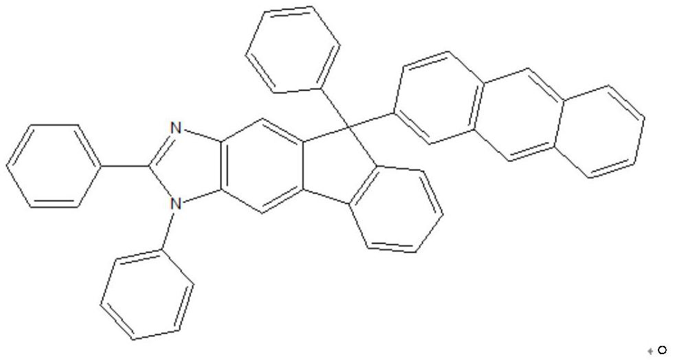
[0051] The synthetic method for preparing compound C is the same as the synthetic method for synthesizing the compound of formula I. The structures of compounds 2, 3, 4, 5 and 6 are

[0052]

[0053]

[0054] The yield of compound C was 79%. Characterization data: melting point (DSC) 302°C, purity 99.9%; 1 H NMR (400MHz, CDCl 3 )δ (ppm): 8.41 (m, 2H), 8.06 (m, 1H), 7.80 (s, 1H), 7.61 (s, 1H), 7.56 (m, 1H), 7.48 (m, 4H), 7.44 ( m,1H),7.32(m,4H),7.30(m,5H),7.24(m,1H),7.22(m,2H),7.14(m,2H),7.08(m,1H),7.06(m ,2H).


PUM

PropertyMeasurementUnit
melting pointaaaaaaaaaa

Abstract

The invention provides an electron transport material, an organic electroluminescent device and a compound with a nitrogen heterocyclic structure. The technical scheme provided by the invention not only has higher stability, but also has high charge transfer capability and high glass transition temperature.

Description

technical field [0001] The invention relates to the field of organic electroluminescent devices, in particular to an electron transport material and an organic electroluminescent device having the same. Background technique [0002] Organic light-emitting diode (Organic Light-Emitting Diode, OLED) is also called organic electro-laser display, organic light-emitting semiconductor. OLED display technology has the advantages of self-illumination, wide viewing angle, almost infinitely high contrast, low power consumption, and extremely high response speed. [0003] Energy level matching is very important for organic electroluminescent devices. Taking a classic organic electroluminescent device as an example, its stacked structure includes: cathode, electron transport layer, light emitting layer, hole transport layer and anode. [0004] Generally, ITO (Indium Tin Oxides, indium tin metal oxide) is used as the anode, but its work function is relatively high, and the energy level ...

Claims


Application Information

Patent Timeline
Patent Type & Authority Applications(China)
IPC IPC(8): C07D235/02C07D403/04C09K11/06H01L51/50H01L51/54
CPCC07D235/02C07D403/04C09K11/06C09K2211/1011C09K2211/1044C09K2211/1059H10K85/615H10K85/654H10K85/6572H10K50/16
Inventor 黄雪明
Owner EVERDISPLAY OPTRONICS (SHANGHAI) CO LTD
Why Eureka
Try Eureka