Photoelectric driving avalanche diode memristor and manufacturing method thereof

An avalanche diode and memristive device technology, which is applied in the field of photoelectric drive avalanche diode memristive devices and their fabrication, can solve the problems of difficult mass production, difficult to be compatible with the application of standard microelectronic process integration, etc., and achieves simple process and convenient operation. Effect

Pending Publication Date: 2021-12-24
HUNAN NORMAL UNIVERSITY
View PDF0 Cites 0 Cited by
  • Summary
  • Abstract
  • Description
  • Claims
  • Application Information

AI Technical Summary

Problems solved by technology

[0002] In the context of the continuous development and innovation of contemporary integrated circuits, the introduction of memristors has greatly promoted the development of artificial intelligence, bionic synapses, and brain-like chips. However, the existing prototypes of memristors are all made of other materials. , it is difficult to be compatible with standard microelectronics technology to achieve large-scale on-chip integration applications. With the passage of time, the research on memristor preparation and characterization testing has become more and more perfect. Computing and other application fields have shown broad application prospects, and will bring powerful transformation capabilities to the future IC field. Silicon-based optical quantum memristors manufactured based on standard CMOS processes will highlight the limitations of traditional computer architectures and study the next generation of quantum computers. The system lays a solid foundation for device prototype and structure
[0003] Most existing memristor prototypes involve transition metal oxide resistive layers, where the formation of conductive filaments and interfacial contact resistance control the memristor behavior, a new type of memristor based on ferroelectric tunnel junction, the device structure schematic diagram and The measured schematic diagram is as figure 1 and figure 2 As shown, the tunneling conductivity can be flexibly tuned in a similar manner by the amplitude and duration of the applied voltage, and the ferroelectric tunneling memristor has a reversible hysteresis nonvolatile resistive switch at room temperature with a high resistance ratio, And the memristive behavior of the device leads to charge redistribution through the electric field at the ferroelectric / electrode interface, thereby regulating the barrier height of the interface. However, it is difficult for the above-mentioned ferroelectric materials to realize memristive devices compatible with standard silicon-based processes for mass production

Method used


Image

  • Photoelectric driving avalanche diode memristor and manufacturing method thereof
  • Photoelectric driving avalanche diode memristor and manufacturing method thereof
  • Photoelectric driving avalanche diode memristor and manufacturing method thereof

Examples


Embodiment Construction

[0030] The present invention will be described in further detail below in conjunction with the accompanying drawings and embodiments. It should be understood that the specific embodiments described here are only used to explain the present invention, not to limit the present invention.

[0031] Unless otherwise defined, all technical and scientific terms used herein have the same meaning as commonly understood by one of ordinary skill in the technical field of the invention. The terms used herein in the description of the present invention are for the purpose of describing specific embodiments only, and are not intended to limit the present invention. As used herein, the term "and / or" includes any and all combinations of one or more of the associated listed items.

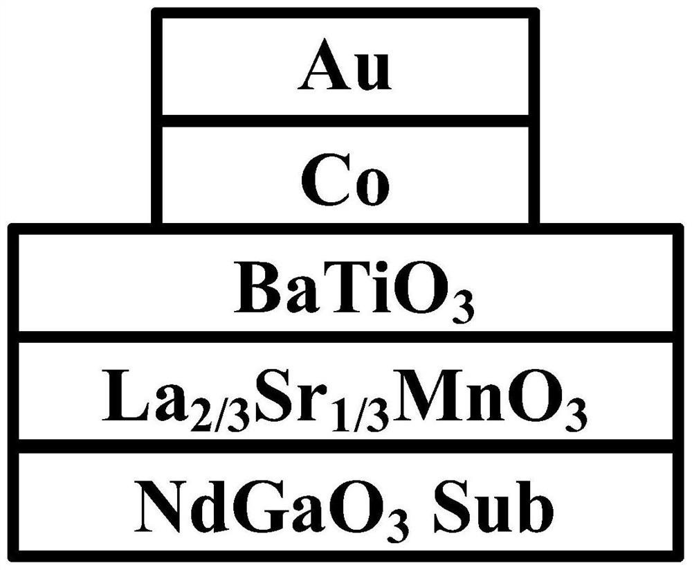
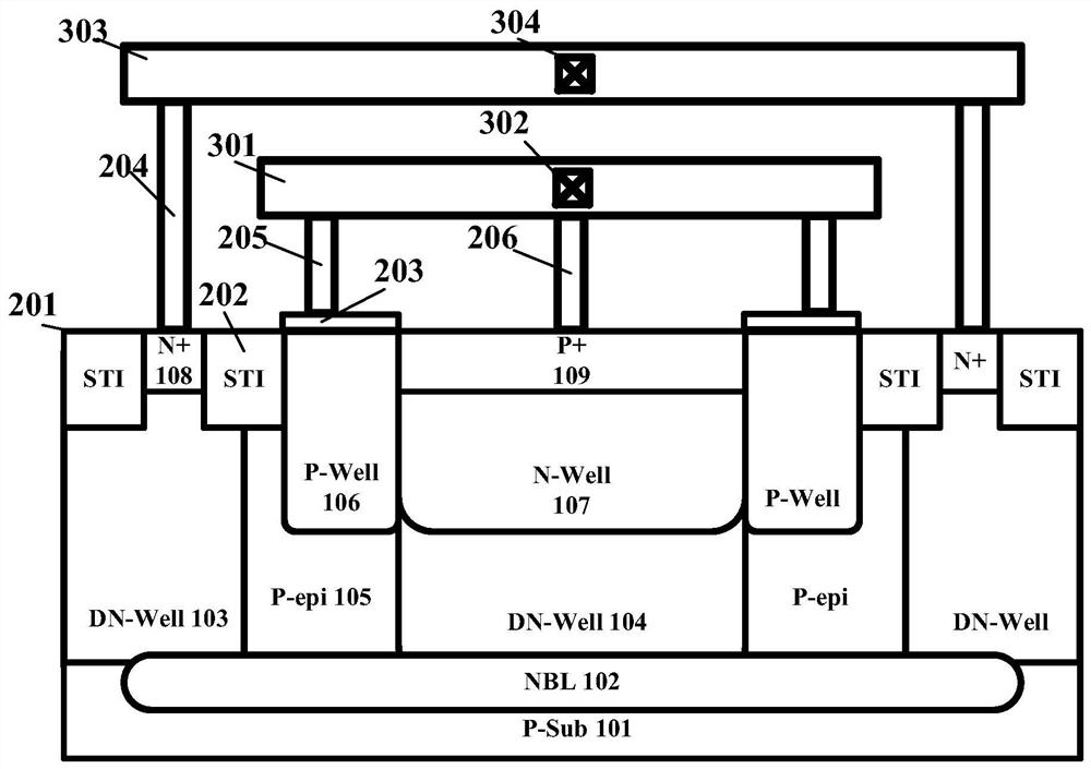
[0032] Such as Figure 3-Figure 6 As shown, a photoelectrically driven avalanche diode memristive device includes a substrate P-Sub101, an NBL region 102, a first ring-shaped DN-Well region 103, a ring-shaped P-e...


PUM


Abstract

The invention discloses a photoelectric driving avalanche diode memristor device and a manufacturing method thereof, a substrate P-Sub is provided with an NBL region, the NBL region is provided with a first annular DN-Well region, the first annular DN-Well region is internally provided with a first annular shallow trench isolation region and an annular N + injection region, and a second annular shallow trench isolation region is located at the junction of the first annular DN-Well region and an annular P-epi region; an annular P-Well region and a polycrystalline silicon ring gate are arranged in the annular P-epi region, an N-Well region is arranged in the second DN-Well region, and a P + injection region is arranged in the N-Well region; the P + injection region is led out to be used as an anode of the photoelectrically driven avalanche diode memristor; the N + injection region is led out to be used as a cathode of the photoelectrically driven avalanche diode memristor; thus, a reverse bias state can be achieved under the condition that periodic pulse signals are applied, the device can be flexibly switched between a high resistance state of a linear region and a low resistance state of an avalanche region through an external bias condition, and therefore a photoelectric controllable memristor mechanism is achieved based on a standard CMOS technology.

Description

technical field [0001] The invention relates to the field of integrated circuits, in particular to a photoelectrically driven avalanche diode memristive device and a manufacturing method thereof. Background technique [0002] In the context of the continuous development and innovation of contemporary integrated circuits, the introduction of memristors has greatly promoted the development of artificial intelligence, bionic synapses, and brain-like chips. However, the existing prototypes of memristors are all made of other materials. , it is difficult to be compatible with standard microelectronics technology to achieve large-scale on-chip integration applications. With the passage of time, the research on memristor preparation and characterization testing has become more and more perfect. Computing and other application fields have shown broad application prospects, and will bring powerful transformation capabilities to the future IC field. Silicon-based optical quantum memri...

Claims


Application Information

Patent Timeline
Patent Type & Authority Applications(China)
IPC IPC(8): H01L45/00H01L27/24
CPCH10B63/20H10N70/20H10N70/841H10N70/011
Inventor 金湘亮汪洋
Owner HUNAN NORMAL UNIVERSITY
Why Eureka
Try Eureka