A silicon-based reconfigurable microwave photonic multi-beamforming network chip

A technology of microwave photonics and network chips, applied in the direction of optical waveguide light guide, optics, light guide, etc., can solve the problems of poor flexibility and practicability, small adjustment accuracy, poor stability, etc., achieve simple structure and control, improve working bandwidth, and size small effect

Active Publication Date: 2022-08-09
SHANGHAI JIAO TONG UNIV
View PDF3 Cites 0 Cited by
  • Summary
  • Abstract
  • Description
  • Claims
  • Application Information

AI Technical Summary

Problems solved by technology

According to different specific applications, the definition of different sub-arrays allows to present up to four spatially multiplexed beams oriented in different directions, limited by the characteristics of discrete devices, its adjustment accuracy is small, and its stability is poor
In terms of integration solutions, in 2021, the research team of Zhejiang University (Opt.Commun., 2021, 489) also adopted the method of dividing sub-arrays to expand the original 2D beamforming scheme to beamforming with multiple beams that can be independently controlled, which is relatively easy to implement However, this solution requires complex connections between multiple chips, and the integration level is low. The maximum number of multi-beam formation and the number of array elements required for single beam formation are fixed, and the back-end also needs to add a microwave power distribution structure. Less flexibility and usability

Method used


Image

  • A silicon-based reconfigurable microwave photonic multi-beamforming network chip
  • A silicon-based reconfigurable microwave photonic multi-beamforming network chip
  • A silicon-based reconfigurable microwave photonic multi-beamforming network chip

Examples


Embodiment Construction

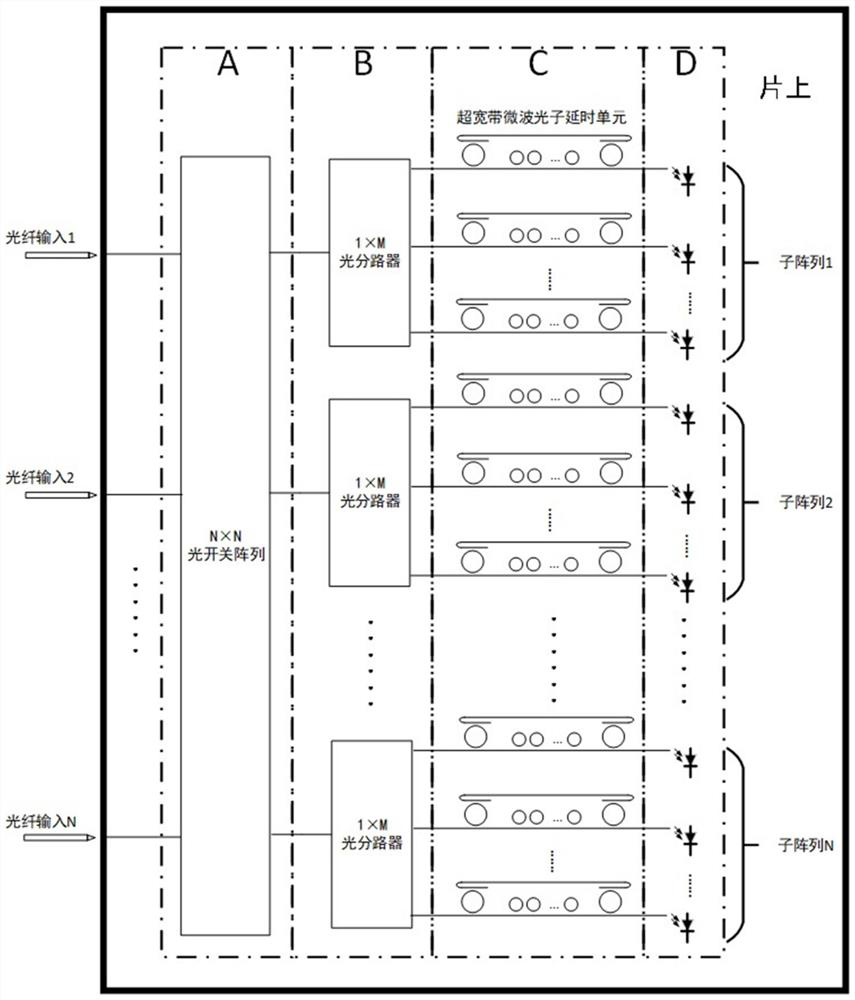
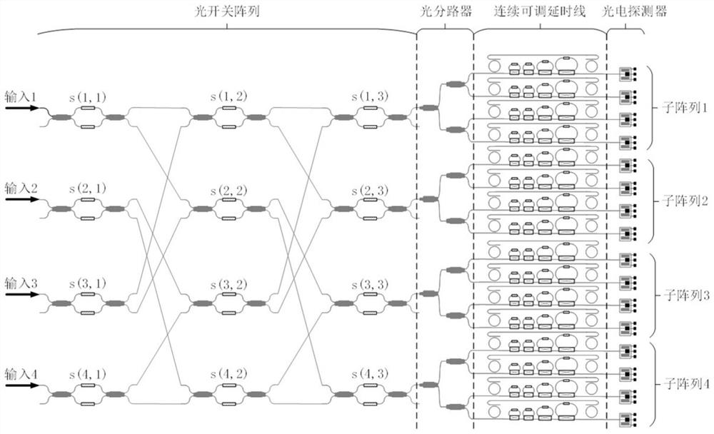
[0033] The present invention realizes a silicon-based reconfigurable microwave photonic multi-beam forming network chip, the overall structure of which is as follows: figure 1 shown. figure 2 The illustrated embodiment is a specific embodiment of the present invention in the case of using a 4×4 optical switch array. The structure specifically includes a 4×4 optical switch array, 4 1×4 optical splitters, 16 ultra-wideband continuously adjustable optical true delay line arrays and 16 detector arrays; the input signals of the 4 fiber couplers are 4 The carrier wavelength of the channel is λ, and the modulation signal is a single-sideband modulated optical signal of the microwave signal to be transmitted. The output ends of the four fiber couplers are respectively connected with the four input ends of the 4×4 optical switch array. The four output ends of the ×4 optical switch array are respectively connected with the input ends of the four 1×4 optical splitters, and the output e...


PUM


Abstract

The invention relates to a silicon-based reconfigurable microwave photonic multi-beam forming network chip, comprising an optical fiber coupler, an optical switch array, an optical splitter, an ultra-wideband continuously adjustable optical true delay line array and a detector array; the optical fiber The coupler is used to input the single-sideband modulated optical signal of the microwave photonic phased array radar, the optical switch array and the optical splitter are used for the reconstruction of the number of array elements used to form the microwave photon multi-beam and the microwave photon single beam, the ultra-wideband A continuously adjustable optical true delay line array is used to independently adjust the delay on each microwave array element, and the detector array is used to output microwave signals. The beneficial effect is that it is used for microwave photonic phased array radar, and realizes large instantaneous bandwidth, high resolution, and reconfigurable microwave photon multi-beam forming.

Description

【Technical field】 [0001] The invention relates to the technical field of integrated microwave photonics, in particular to a silicon-based reconfigurable microwave photonic multi-beam forming network chip. 【Background technique】 [0002] Ordinary phased array radar is a phase-controlled electronically scanned array radar, which uses a large number of individually controlled small antenna units arranged into an antenna array. Each antenna unit is controlled by an independent phase-shifting unit. By controlling the phase of the signal transmitted by each antenna unit , the interference pattern of the signals transmitted by each antenna unit in space can be changed, so as to control the direction of beam transmission. The electromagnetic waves emitted by each antenna element of the phased array are synthesized into a radar main lobe beam whose emission direction is close to straight through interference, and the inhomogeneity of each antenna element will form side lobes. Phased...

Claims


Application Information

Patent Timeline
Patent Type & Authority Patents(China)
IPC IPC(8): G02B6/12
CPCG02B6/12G02B2006/12147G02B2006/1215G02B2006/12145
Inventor 陆梁军倪子恒周林杰陈建平刘娇
Owner SHANGHAI JIAO TONG UNIV
Why Eureka
Try Eureka