Deep-shallow combined Schottky barrier tunnel transistor and manufacturing method thereof

A technology of tunnel transistor and Schottky potential, which is applied in the deep and shallow combined Schottky barrier tunnel transistor and its manufacturing field, can solve the problems of large static power consumption, high sub-threshold swing, large leakage, etc. consumption, suppression of reverse leakage current, suppression of the effects of large

Active Publication Date: 2022-01-18
SHENYANG POLYTECHNIC UNIV
View PDF4 Cites 0 Cited by
  • Summary
  • Abstract
  • Description
  • Claims
  • Application Information

AI Technical Summary

Problems solved by technology

[0004] Aiming at the problems of high sub-threshold swing, large static power consumption, and large leakage current existing in current tunneling transistor technology and Schottky barrier transistor technology, the present invention provides a deep-shallow combination Schottky barrier tunnel transistor and its manufacture method

Method used


Image

  • Deep-shallow combined Schottky barrier tunnel transistor and manufacturing method thereof
  • Deep-shallow combined Schottky barrier tunnel transistor and manufacturing method thereof
  • Deep-shallow combined Schottky barrier tunnel transistor and manufacturing method thereof

Examples


Embodiment

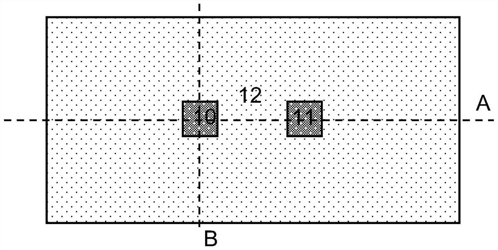
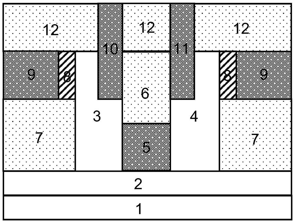
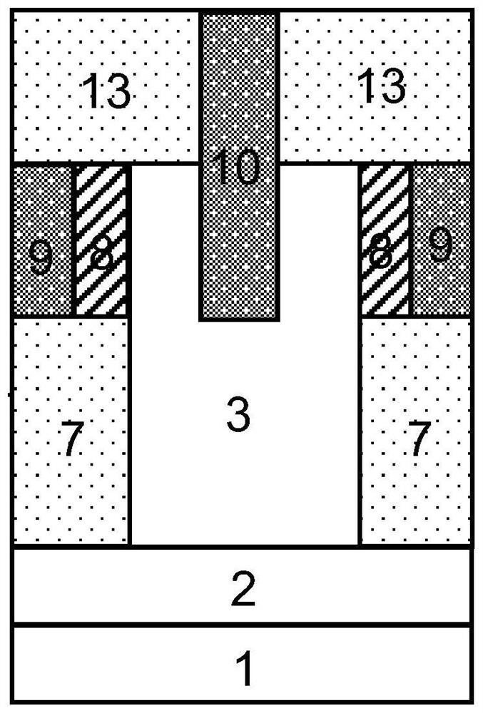
[0054] A deep and shallow combined Schottky barrier tunnel transistor, comprising a silicon substrate 1 of an SOI wafer, a substrate insulating layer 2 of the SOI wafer above the silicon substrate 1 of the SOI wafer, and a substrate insulating layer of the SOI wafer Above 2 are single crystal silicon film a3, single crystal silicon film b4, central metal region 5 and embedded dielectric barrier layer 6; wherein, single crystal silicon film a3 and single crystal silicon film b4 have an impurity concentration lower than 10 16 cm -3 single crystal silicon semiconductor material; the central metal region 5 is located at the bottom between the single crystal silicon film a3 and the single crystal silicon film b4; the left and right sides of the central metal region 5 are respectively connected to the single crystal silicon film a3 and the single crystal silicon films b 4 are in contact with each other;

[0055] For the deep-shallow combined Schottky barrier tunnel transistor used...


PUM


Abstract

The invention discloses a deep-shallow combined Schottky barrier tunnel transistor and a manufacturing method thereof, and an N-type deep-shallow combined Schottky barrier tunnel transistor. According to the invention, a deep Schottky barrier is formed between a central metal region and a valence band of a monocrystalline silicon thin film, so that a large number of holes in the monocrystalline silicon thin film close to a source electrode cannot pass through the central metal region to form continuous current, and static power consumption and generation of a large number of reverse leakage current are effectively restrained; in a sub-threshold region, a deep Schottky barrier formed between the conduction band of the monocrystalline silicon thin film and the source electrode effectively inhibits electrons from the source electrode from being injected into the monocrystalline silicon thin film through a hot electron emission effect, so that generation of sub-threshold current is effectively inhibited; and compared with a current tunneling transistor technology and a Schottky barrier transistor technology, the device of the invention has the characteristics of low subthreshold swing, low static power consumption, low electric leakage, avoidance of a doping process and a millisecond-level heat treatment process in a manufacturing process, compatibility of a logic function and a current CMOS integrated circuit and the like.

Description

technical field [0001] The invention belongs to the technical field of integrated circuit design and manufacture, and in particular relates to a deep-shallow combined Schottky barrier tunnel transistor suitable for high integration, low power consumption, and high-performance integrated circuit design and manufacture and a manufacturing method thereof. Background technique [0002] The basic unit of integrated circuits, MOSFETs, is limited by the physical mechanism of its own current generation during operation, and its subthreshold swing cannot be lower than 60mV / dec. In order to improve the sub-threshold characteristics of the basic unit of integrated circuits and reduce static power consumption, tunnel transistors have been proposed. However, both MOSFETs and tunnel transistors require doping processes to form N-type or P-type source and drain regions. To achieve this, for nanoscale integrated circuits, it is necessary to develop a millisecond-level heat treatment process...

Claims


Application Information

Patent Timeline
Patent Type & Authority Applications(China)
IPC IPC(8): H01L29/78H01L21/336
CPCH01L29/7839H01L29/66477
Inventor 刘溪李萌萌
Owner SHENYANG POLYTECHNIC UNIV
Why Eureka
Try Eureka