Micro-ring optical switch based on three-dimensional integration of silicon-silicon nitride

A silicon nitride microring and three-dimensional integration technology, applied in the field of optical switches, can solve the problems of not fully utilizing the optical switch design scheme, immature implementation scheme, and failure to reflect advantages, etc., to achieve easy expansion, improve thermal tuning efficiency, The effect of simple structure

Active Publication Date: 2022-08-09
SHANGHAI JIAOTONG UNIV
View PDF6 Cites 0 Cited by
  • Summary
  • Abstract
  • Description
  • Claims
  • Application Information

AI Technical Summary

Problems solved by technology

Researchers from Japan Advanced Industrial Research Institute and Columbia University have successively reported optical switches based on silicon-silicon nitride integrated platforms, but it is difficult to achieve low-loss waveguide intersection and high-efficiency interlayer at the same time because only one layer of silicon nitride waveguide is used. Transmission, failed to reflect the advantages
[0005] The emergence of a multi-layer silicon nitride integrated platform is very beneficial to solve many problems of large-scale optical switches, but the existing implementation schemes are still immature, and there is no optical switch design scheme that fully utilizes the advantages of this integrated platform for the time being

Method used


Image

  • Micro-ring optical switch based on three-dimensional integration of silicon-silicon nitride
  • Micro-ring optical switch based on three-dimensional integration of silicon-silicon nitride
  • Micro-ring optical switch based on three-dimensional integration of silicon-silicon nitride

Examples


Embodiment Construction

[0026] The following examples are further explained to the present invention. This instance is only used to explain the invention in detail, and it cannot be understood as a limit on the scope of protection of the present invention.

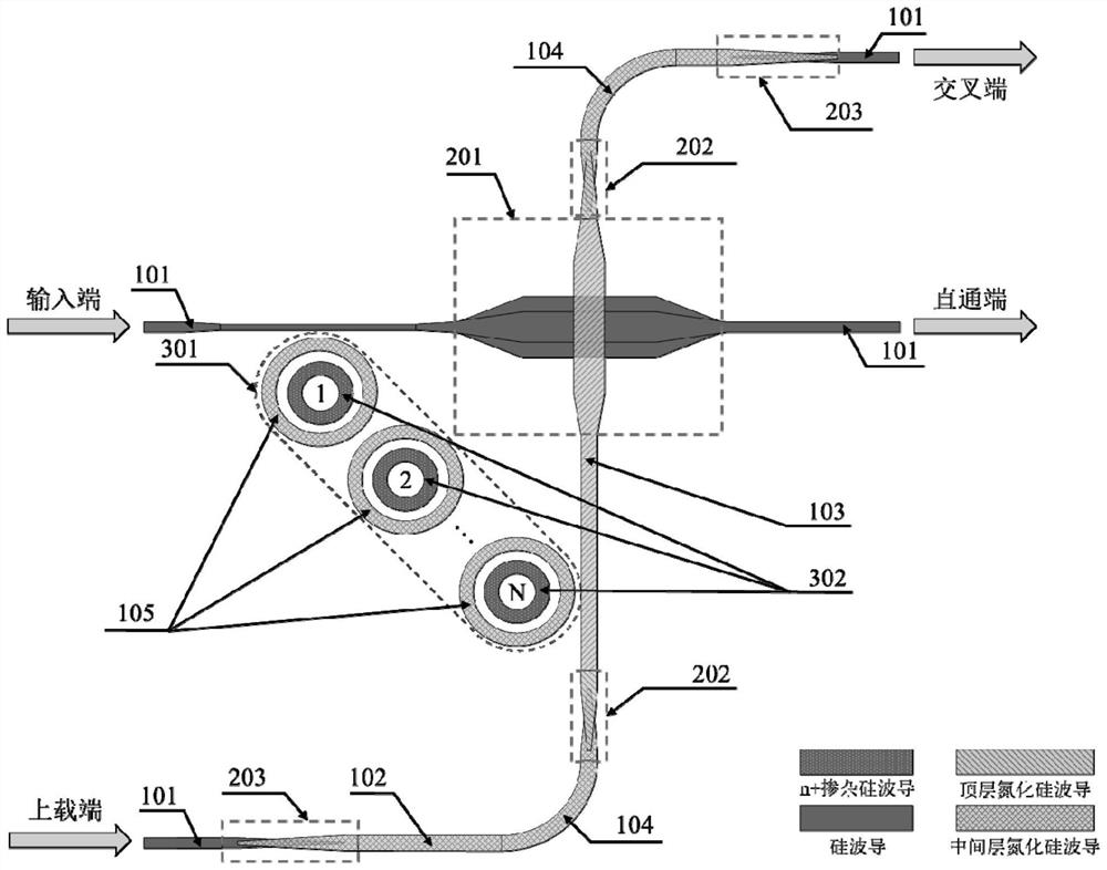
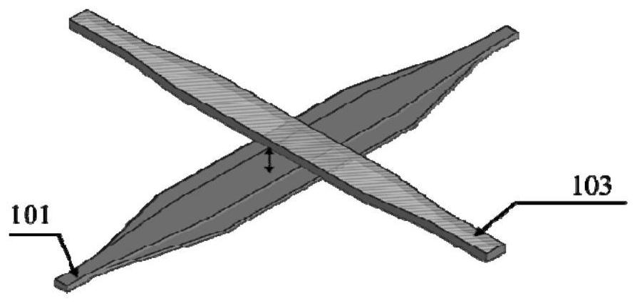
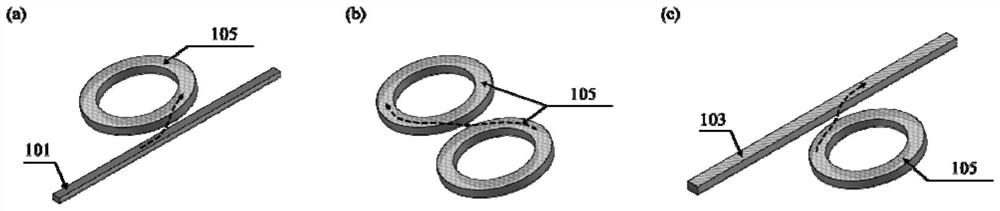
[0027] like figure 1 It shows that the present invention proposes a micro-circular switch based on silicon-silicon nitride-based three-dimensional integration. Two -layer silicon nitride waveguide (102, 103) is integrated on the silicon waveguide (101), and the silicon waveguide (101) is discharged horizontally by silicon waveguide (101) between the waveguide. The ranking, forming a three -dimensional wave interface (201); one end of the silicon waveguide (101) as the input end of the light signal, and the other end as the direct end; Polida (104), composed of silicon nitride microcirculation (105) with 360 ° bending; one end of the top layer of silicon nitride (103) through silicon nitrite-silicon nainer wave guide intercourse (202) and silicon nitr...


PUM


Abstract

A micro-ring optical switch based on three-dimensional integration of silicon-silicon nitride. A three-dimensional waveguide cross junction is formed by a laterally arranged silicon waveguide and a longitudinally arranged top layer silicon nitride waveguide, and is cascaded with a middle layer of silicon nitride waveguides. Microrings are formed by vertical coupling. The interlayer coupler is used to realize the interlayer coupling between the silicon nitride waveguide in the middle layer and the other two layers of waveguides, so as to assist the conversion of optical signals between the three layers of waveguides. The invention utilizes the doping of the bottom silicon waveguide to form a micro-heater, and generates heat by applying electricity at both ends of the doped waveguide to adjust the resonance wavelength of the silicon nitride microring of the intermediate layer, and switches the path of the optical signal, and has the advantages of low power consumption . When the wavelength of the optical signal matches the resonant wavelength of the microring, two optical signals in opposite directions can be routed in the device simultaneously. The optical switch structure of the present invention has a large processing tolerance, does not require additional power consumption to compensate for the shift of the operating wavelength, is insensitive to temperature, and does not require a complex control circuit.

Description

Technical field [0001] The invention involves the field of optical switching technology, which is specifically involved a microcircular light switch based on silicon-silicon nitrite. Background technique [0002] The advent of the era of big data has promoted the rapid development of high -speed data transmission in the field of long -distance communication links, short -distance data centers, high -performance computing systems, and even the light interconnection between chips and chips. With the increase in data rates in the data center cluster switch, the existing electric switching system is facing challenges such as power consumption and delay. Communication connection. As a key part of the optical connection network, the development of high -speed, low -loss, low power consumption, and high transmission bandwidth of the light switch is of great significance for the development of the future data center network. The manufacturing process of silicon -based photonic devices is...

Claims


Application Information

Patent Timeline
Patent Type & Authority Patents(China)
IPC IPC(8): G02B6/12G02B6/125
CPCG02B6/12G02B6/12002G02B6/125G02B2006/12038G02B2006/12145
Inventor 陆梁军李鑫高伟周林杰陈建平
Owner SHANGHAI JIAOTONG UNIV
Why Eureka
Try Eureka