Total dose irradiation resistant SOI (Silicon On Insulator) device and preparation method thereof

An anti-total dose, device technology, applied in the direction of electric solid devices, semiconductor devices, semiconductor/solid device components, etc., can solve the problems of limited protection ability, complex coating process, lead toxicity, etc., to achieve excellent structural characteristics, simplification Preparation process, shielding effect of total dose effect

Active Publication Date: 2022-01-28
HARBIN INST OF TECH
View PDF5 Cites 1 Cited by
  • Summary
  • Abstract
  • Description
  • Claims
  • Application Information

AI Technical Summary

Problems solved by technology

[0003] At present, the total dose effect shielding is usually completed by metals such as lead or materials alternately laminated with some low-Z metals. However, due to its high density and high mass, lead increases the load of the overall structure in some applications. At the same time, lead has certain toxicity and is harmful to humans and the environment.
However, the current high-low-Z alternate lamination coating process is complex, requiring multiple coatings and drying, which takes a long time and has limited protection capabilities.
Moreover, another limitation of the materials currently used is that they basically have a certain shape and strength, and it may not be possible to achieve some flexibility if they want to

Method used


Image

  • Total dose irradiation resistant SOI (Silicon On Insulator) device and preparation method thereof
  • Total dose irradiation resistant SOI (Silicon On Insulator) device and preparation method thereof
  • Total dose irradiation resistant SOI (Silicon On Insulator) device and preparation method thereof

Examples


Embodiment 1

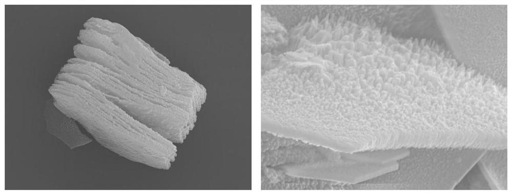
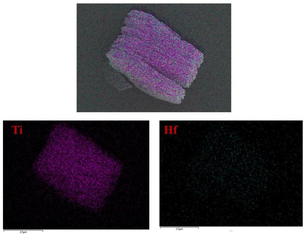
[0044] Use method 1 (hydrofluoric acid etching) to complete Mxene etching, then transfer Mxene to the chamber of the atomic layer deposition device, and perform high-Z metal oxide HfO on it 2 Coating modification. The reaction temperature should be controlled at 200°C, the pressure should be controlled at 0.155torr during the reaction, and the source of high Z metal oxides is [(CH 3 )C 2 h 5 )N] 4 Hf, the pulse time is 0.15s, and the reaction time is 6s. After the pulse and reaction are completed, use high-purity nitrogen (99.999%) to purge the residual reactants and by-products in the pipeline and cavity for 60s. Then high-purity water is used as the oxygen source, the pulse time is 0.015s, and the reaction time is 6s. After the pulse reaction is completed, the residual reactants and by-products in the pipeline and cavity are purged with high-purity nitrogen (99.999%) for 60s. The high-Z metal oxide source and the oxygen source are alternately fed into the reaction chambe...

Embodiment 2

[0047] Example 2: Using method 2 (HCl+LiF etching) to complete Mxene etching, then transfer Mxene to the chamber of the atomic layer deposition device, and perform high-Z metal oxide HfO on it 2 Coating modification. The reaction temperature should be controlled at 150°C, the pressure should be controlled at 0.155torr during the reaction, and the source of the high Z metal oxide is [(CH 3 )C 2 h 5 )N] 4 Hf, the pulse time is 0.15s, and the reaction time is 6s. After the pulse and reaction are completed, use high-purity nitrogen (99.999%) to purge the residual reactants and by-products in the pipeline and cavity for 60s. Then high-purity water is used as the oxygen source, the pulse time is 0.015s, and the reaction time is 6s. After the pulse reaction is completed, the residual reactants and by-products in the pipeline and cavity are purged with high-purity nitrogen (99.999%) for 60s. The high-Z metal oxide source and the oxygen source are alternately fed into the reaction ...

Embodiment 3

[0049] Example 3: Using method 3 (NaOH hydrothermal etching) to complete Mxene etching, then transfer Mxene to the chamber of the atomic layer deposition device, and perform high-Z metal oxide HfO on it 2 Coating modification. The reaction temperature should be controlled at 180°C, the pressure should be controlled at 0.155torr during the reaction, and the source of the high Z metal oxide is [(CH 3 )C 2 h 5 )N] 4 Hf, the pulse time is 0.15s, and the reaction time is 6s. After the pulse and reaction are completed, use high-purity nitrogen (99.999%) to purge the residual reactants and by-products in the pipeline and cavity for 60s. Then high-purity water is used as the oxygen source, the pulse time is 0.015s, and the reaction time is 6s. After the pulse reaction is completed, the residual reactants and by-products in the pipeline and cavity are purged with high-purity nitrogen (99.999%) for 60s. The high-Z metal oxide source and the oxygen source are alternately fed into the...


PUM


Abstract

The invention discloses a total dose irradiation resistant SOI device and a preparation method thereof, and belongs to the field of radiation protection materials. The problems that an existing high-low Z alternate laminated coating process is complex, multiple times of coating and drying are needed, consumed time is long, and the protection capacity is limited are solved. And the technical problem that flexibility cannot be realized is solved. The preparation method comprises the following steps: etching an MAX-phase ceramic matrix to obtain a Ti3C2Tx material with a layered structure, depositing high-Z metal into the Mxene layered structure through an atomic layer deposition technology to obtain a composite material, mixing the composite material with a resin matrix, and coating the mixture on the surface of an SOI device to obtain a radiation protection coating. The material disclosed by the invention can be used in the fields of radiation-proof clothes in life, medical treatment and protection required in nuclear reaction.

Description

technical field [0001] The invention belongs to the field of radiation protection materials; in particular, it relates to an SOI device capable of resisting total dose radiation and a preparation method thereof. Background technique [0002] The total dose effect refers to the degradation of device performance caused by the trapped charges induced in the oxide layer by radiation. For SOI devices, radiation not only generates trap charges and interface state charges in the gate oxide, but also in other dielectrics such as field isolation oxides and buried oxides. These radiation-induced charges will increase the off-state leakage and edge leakage of the device, resulting in increased static power consumption and even functional failure of the integrated circuit. Therefore, only by solving the problem of anti-total dose hardening of SOI materials and devices, can we remove obstacles for the military application of SOI technology and better apply it in anti-radiation hardened ...

Claims


Application Information

Patent Timeline
Patent Type & Authority Applications(China)
IPC IPC(8): H01L23/552G21F1/02G21F1/12
CPCH01L23/552G21F1/02G21F1/12
Inventor 吴晓宏李杨秦伟卢松涛洪杨
Owner HARBIN INST OF TECH
Why Eureka
Try Eureka