Epitaxial structure of UVB chip and UVB chip

An epitaxial structure and chip technology, applied in nanotechnology, electrical components, nanotechnology, etc. for materials and surface science, can solve problems such as affecting luminous efficiency, increasing material defect density, and poor surface quality

Pending Publication Date: 2022-02-18
ZHIXIN SEMICON (HANGZHOU) CO LTD
View PDF11 Cites 2 Cited by
  • Summary
  • Abstract
  • Description
  • Claims
  • Application Information

AI Technical Summary

Problems solved by technology

At the same time, in order to ensure the blocking effect of electrons, the Al composition of the quantum barrier and the electron blocking layer AlInGaN is kept at more than 50%, which will inevitably lead to a large difference in the Al composition of the quantum well AlInGaN layer and other AlInGaN layers, so that in the quantum luminescence There is a very large difference in lattice constant between layers in the layer
The large difference in lattice constant between layers leads to a series of serious consequences. The large difference in lattice constant between layers will first lead to a very large stress in the material body, which will lead to the quantum Stark effect, making the internal Quantum efficiency is low
At the same time, too much difference in lattice constant between layers will lead to poor surface quality and rough surface, which is also an important factor affecting efficiency, and therefore it is difficult to process into chips
What's more, because the Al composition of the UVB quantum well is relatively low, and the Ga composition is relatively high, because the migration rate of Al atoms and Ga atoms during the growth process is very different, which will lead to low Al composition UVB There are obvious differences in the growth of the quantum well AlInGaN layer and the high Al composition UVB quantum barrier AlInGaN layer
And because the migration of Ga atoms is too fast during the growth process of the low Al composition UVB quantum well AlInGaN layer, it is easy to form high-density GaN hexagonal defects, which will lead to a rapid increase in the defect density inside the material and affect the luminous efficiency.

Method used


Image

  • Epitaxial structure of UVB chip and UVB chip
  • Epitaxial structure of UVB chip and UVB chip
  • Epitaxial structure of UVB chip and UVB chip

Examples


preparation example Construction

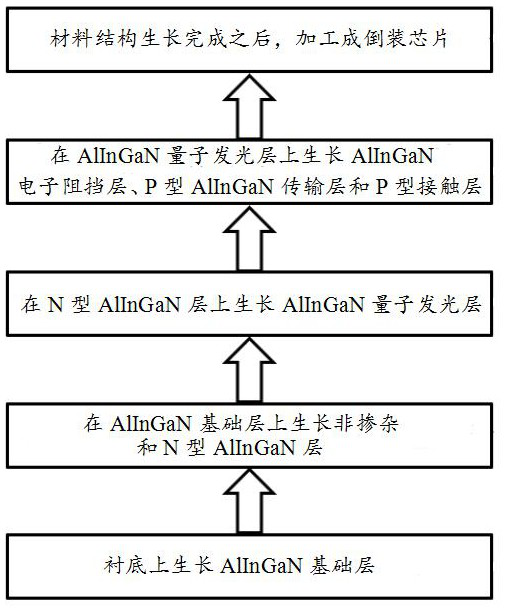
[0068] In the present invention, the preparation method of the epitaxial structure of the UVB chip, according to figure 1 The shown process preferably includes the following steps:

[0069] An AlInGaN base layer, a non-doped AlInGaN layer, an N-type AlInGaN layer, an AlInGaN quantum luminescent layer, an AlInGaN electron blocking layer, a P-type AlInGaN transport layer and a P-type contact layer are sequentially grown on the upper surface of the substrate to obtain the UVB chip. epitaxial structure.

[0070] Before the epitaxial structure is grown on the upper surface of the substrate, the substrate is preferably pretreated, and the pretreatment includes sequential baking and cleaning; in the present invention, the baking is preferably performed after the The substrate is placed in a reactor and baked at 1050°C in a hydrogen atmosphere. The present invention does not have any special restrictions on the cleaning process. It is carried out by a process well known to those skil...

Embodiment 1

[0095] Put the sapphire substrate into the MOCVD equipment, pass through hydrogen gas, and after baking at 1050°C, clean the oxides and impurities on the surface of the sapphire substrate;

[0096] At a temperature of 1300 ° C, AlN layers (thickness 3 μm) were grown sequentially on the surface of the cleaned sapphire substrate, AlN layers (thickness 2 nm) and Al 0.8 Ga 0.2 N layer (thickness 4nm) 20 cycles, growth of non-doped Al 0.65 Ga 0.35 N layer (thickness 1μm), grow N-type doped Al 0.65 Ga 0.35N layer (thickness 0.5μm, N-type Si doping concentration 8×10 18 cm -3 ), growing N-type doped Al 0.5 Ga 0.5 N layer (thickness 0.5μm, N-type Si doping concentration 1.5×10 19 cm -3 ), growing Al 0.5 In 0.01 Ga 0.49 N quantum barrier layer (thickness 12nm), grown Al 0.2 In 0.01 Ga 0.79 N quantum well layer (thickness 2nm), in which the Al 0.5 In 0.01 Ga 0.49 N quantum barrier layer and Al 0.2 In 0.01 Ga 0.79 A lattice strain layer (Al x Ga 1-x N layer, with x...

Embodiment 2

[0103] Put the sapphire substrate into the MOCVD equipment, pass through hydrogen gas, and after baking at 1050°C, clean the oxides and impurities on the surface of the sapphire substrate;

[0104] At a temperature of 1250 ° C, AlN layers (2 μm in thickness) were grown sequentially on the surface of the cleaned sapphire substrate, AlN layers (2 nm in thickness) and Al 0.8 Ga 0.2 N layer (thickness 2nm) 50 cycles, growth of non-doped Al 0.6 Ga 0.4 N layer (thickness 1μm), grow N-type doped Al 0.6 Ga 0.4 N layer (thickness 0.6μm, N-type Si doping concentration 5×10 18 cm -3 ), growing N-type doped Al 0.45 Ga 0.55 N layer (thickness 0.5μm, N-type Si doping concentration 1×10 19 cm -3 ), growing Al 0.45 In 0.01 Ga 0.54 N quantum barrier layer (thickness 5nm), grown Al 0.2 In 0.01 Ga 0.79 N quantum well layer (thickness 3nm), in which the Al 0.45 In 0.01 Ga 0.54 N quantum barrier layer and Al 0.2 In 0.01 Ga 0.79 A lattice strain layer (Al x Ga 1-x N layer, x ...


PUM

PropertyMeasurementUnit
thicknessaaaaaaaaaa
thicknessaaaaaaaaaa
thicknessaaaaaaaaaa

Abstract

The invention relates to the technical field of ultraviolet light emitting diode chips, and particularly relates to an epitaxial structure of a UVB chip and the UVB chip. The lattice strain layer is arranged between the Alx1Iny1Ga1-x1-y1N quantum barrier layer with the high Al component and the Alx2Iny2Ga1-x2-y2N quantum well layer with the low Al component to play a role in connection and transition, and the problem of a large stress caused by a large lattice constant difference is efficiently solved; and meanwhile, the Al content in the lattice strain layer is between x1 and x2 so that the problem of high defect density caused by sudden and too fast migration of Ga is avoided, and the luminous efficiency is further improved.

Description

technical field [0001] The invention relates to the technical field of ultraviolet light emitting diode chips, in particular to an epitaxial structure of a UVB chip and a UVB chip. Background technique [0002] According to the survey by the Chinese Medical Association, the number of people with calcium deficiency in my country is as high as 900 million, and the number of people with severe calcium deficiency has reached 200 million, especially infants, pregnant women and the elderly. Calcium deficiency can cause more than one hundred diseases in the eight major systems, among which osteoporosis is the most. At present, there are about 90 million osteoporosis patients in my country, ranking seventh among common diseases and frequently-occurring diseases. The overall prevalence rate in mainland China is 12.4%, and the prevalence rate among the elderly is more than 50%, among which the incidence rate of fracture is close to 1 / 3. Therefore, how to supplement calcium has becom...

Claims


Application Information

Patent Timeline
Patent Type & Authority Applications(China)
IPC IPC(8): H01L33/12H01L33/06H01L33/32B82Y30/00B82Y40/00
CPCH01L33/12H01L33/06H01L33/32B82Y30/00B82Y40/00
Inventor 黄小辉倪逸舟
Owner ZHIXIN SEMICON (HANGZHOU) CO LTD
Why Eureka
Try Eureka