Nitrogen-containing compound, organic electroluminescent device comprising same and electronic device

A technology of nitrogen compounds and chemical bonds, applied in the field of organic electroluminescent devices and electronic devices, to achieve excellent electron injection and transport characteristics, enhance the balance degree, and improve the effect of electron transport performance

Active Publication Date: 2022-02-22
SHAANXI LTMS OPTOELECTRONICS MATERIAL CO LTD
View PDF3 Cites 1 Cited by
  • Summary
  • Abstract
  • Description
  • Claims
  • Application Information

AI Technical Summary

Problems solved by technology

In the existing organic electroluminescent devices, the most important problem is life and efficiency. With the large area of ​​the display, the driving voltage is also increased, and the luminous efficiency and power efficiency also need to be improved, and a certain service life must be guaranteed. Therefore, organic materials must solve these efficiency or lifetime problems, and it is necessary to continuously develop new materials for organic light-emitting devices with high efficiency, long life, and suitable for mass production.

Method used


Image

  • Nitrogen-containing compound, organic electroluminescent device comprising same and electronic device
  • Nitrogen-containing compound, organic electroluminescent device comprising same and electronic device
  • Nitrogen-containing compound, organic electroluminescent device comprising same and electronic device

Examples


Embodiment 1

[0229] Green Organic Electroluminescent Devices

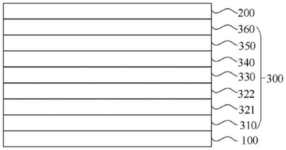
[0230] The anode is formed with indium tin oxide (ITO) on the substrate on which the reflective layer is formed, with a thickness of Cut into a size of 40mm×40mm×0.7mm, and prepare it into an experimental substrate with cathode, anode and insulating layer patterns by photolithography process, and clean the surface of ITO substrate with organic solvent to remove impurities on the surface; or use ultraviolet Ozone and O 2 :N 2 Plasma surface treatment to increase the work function of the anode.

[0231] Vacuum-evaporate PtPC on the anode of the substrate by PVD method to form a thickness of the hole injection layer, and the hole injection layer is evaporated The HT-01 forms the hole transport layer.

[0232] Evaporation on the hole transport layer The HT-02 forms a hole assisting layer.

[0233] On the hole assisting layer, compound A-1-1:GH-P:Ir(3mppy) 3 Co-evaporated at a ratio of 45%: 45%: 10%, forming a thickness ...

Embodiment 2-28

[0237] When forming the green light-emitting layer, the compounds shown in Table 11 were used instead of the compound A-1-1 in Example 1, and the organic electroluminescent device was fabricated by the same method as in Example 1.

Embodiment 29

[0253] Set the ITO thickness to The substrate was cut into a size of 40mm×40mm×0.7mm, and the photolithography process was used to prepare the experimental substrate with cathode, anode and insulating layer patterns, using ultraviolet ozone and O 2 :N 2 The plasma is used for surface treatment to remove surface particles and improve the anode work function.

[0254] Vacuum evaporation of PtPC on the substrate by PVD method to form a thickness of The hole injection layer, and HT-01 is evaporated on the hole injection layer to form a thickness of hole transport layer.

[0255] The thickness of evaporation on the hole transport layer is HT-02, forming a hole-assisting layer.

[0256] On the hole assisting layer, compound RH-P: Compound A-1-26: Ir(dmpq) 2 acac is co-evaporated at the ratio of 49%: 49%: 2% (evaporation rate), forming The organic electroluminescent layer (red emitting layer).

[0257] BCP and LiQ were mixed at a weight ratio of 1:1 and evaporated to for...


PUM


Abstract

The invention provides a nitrogen-containing compound, an organic electroluminescent device thereof and an electronic device, and belongs to the technical field of organic electroluminescence. The structural general formula of the nitrogen-containing compound is represented by a formula 1, and the nitrogen-containing compound is applied to the organic electroluminescent device and can remarkably improve the performance of the organic electroluminescent device.

Description

technical field [0001] The present application relates to the field of organic electroluminescent technology, in particular, to a nitrogen-containing compound and an organic electroluminescent device and electronic device containing the same. Background technique [0002] As a new generation of display technology, organic electroluminescent materials (OLED) have the advantages of ultra-thin, self-luminous, wide viewing angle, fast response, high luminous efficiency, good temperature adaptability, simple production process, low driving voltage, and low energy consumption. It has been widely used in industries such as flat panel display, flexible display, solid state lighting and vehicle display. [0003] The organic electroluminescence phenomenon refers to a phenomenon in which electrical energy is converted into light energy using an organic material. An organic electroluminescent device utilizing the phenomenon of organic electroluminescence generally has a structure inclu...

Claims


Application Information

Patent Timeline
Patent Type & Authority Applications(China)
IPC IPC(8): C07D487/04C07F7/08H01L51/54H01L51/50
CPCC07D487/04C07F7/0812H10K85/622H10K85/615H10K85/654H10K85/6576H10K85/6574H10K85/40H10K85/6572H10K50/11
Inventor 马天天呼琳琳金荣国杨雷
Owner SHAANXI LTMS OPTOELECTRONICS MATERIAL CO LTD
Why Eureka
Try Eureka